Oh - and the template punchthrough works GREAT too. Super idea. So much easier than just referencing a piece of paper nearby.
↧
ESP32S-HiLetgo Dev Boad with Pinout Template
↧
Help for part MDD10A
https://drive.google.com/folderview?id=0B71jedkH0IPRdDV3NUFacFJsY1E&usp=sharing
See this link from Cytron’s official website. You can get every Cytron’s fritzing boards.
↧
↧
Need Help with a DC-DC Buck Converter (LM2596) and LI-ION Batteries
Hello!
I am new to Fritzing and I would need some help with creating or importing 2 parts:
- LM2596 DC to DC Buck Converter
- Li-Ion Batteries 3.7 2500 mAh
↧
Need Help with a DC-DC Buck Converter (LM2596) and LI-ION Batteries
Both are available in the core parts library. If they hadn’t been the place to start is a google search of the form “fritzing part lipo battery” which will turn up parts that people have made.


Peter
↧
Need Help with a DC-DC Buck Converter (LM2596) and LI-ION Batteries
Does it depend if I have the cracked version? Because I do not find LM2596.
I find the batteries but what do I have to do if I need to change the voltage or the current value?
↧
↧
Need Help with a DC-DC Buck Converter (LM2596) and LI-ION Batteries
I’m not sure what a cracked version is, but no it shouldn’t matter. You may have to update the parts library (it should happen automatically, but in some circumstances it doesn’t.) First try Help->check for updates to see what it says. If that doesn’t work you need to manually update the parts db. Note you need to find the Fritzing install directory on your system and load the github repository in to the Fritzing parts directory.
As to the batteries once you have dragged it in to a sketch (not in the parts bin!). Inspector will change some things. If what you want isn’t changeable then you (or more likely one of us) would need to make a custom part.

In Inspector (lower right circled in red) you can change amp hour ratings to some common values.
Peter
↧
Need Help with a DC-DC Buck Converter (LM2596) and LI-ION Batteries
Thank you very much!I love you man! It was very sceptic about the reply time on the forum! Now I have my LM2596 and I can continue my faculty license project! I hope I will not need assistance anymore but if I go any problem, I will try to solve it and after that I will ask here for some help!
Thank you very much sir and have a great night!
↧
Creating parts with movable schematic elements
(post withdrawn by author, will be automatically deleted in 24 hours unless flagged)
↧
PS2 gamepad port
The Fritzing gods have smiled on you  , some skilled person has posted a svg of the ps2 gamepad under the creative commons licence so I swiped it. There is a female connector available (but no layout information) available from Robotshop here
So this is a full part (bb schematic and pcb) but pcb is likely wrong as the positions were done from a rescaled jpg image. If someone has one of these connectors and will post the size and position of the pins I’ll fix pcb up.
ps2-gamepad.fzpz (11.0 KB)
Peter
↧
↧
New part pads connecting with ground fill
Hey everyone, I’ve done a bunch of digging and no luck on finding a solution for this.
I made a custom part (SK6812 Mini-E LED) that I customized from LED strips I found here. After a lot of trial and error in Inkscape, I got a working part. However, after setting ground fill for my PCB using this part, it fills two of the upper pads in the process and leaves the bottom two unfill (like normal). I spent a couple hours reviewing my files and I don’t see any thing wrong that is obvious.
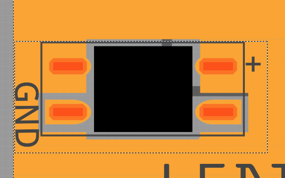
The only thing I found searching the internet, is something about matrix transformations, except I never used any of those, at least not intentionally. I attached the file. Thanks for any help!
SK6812 Mini-E RGB LED .fzpz (11.6 KB)
↧
New part pads connecting with ground fill
I ran your part through FritzingCheckPart.py and it has a number of complaints.
“This is a through hole part as both copper0 and copper1 views are present.
If you wanted a smd part remove the copper0 definition from line 47”
except this is a SMD part and thus copper0 should not be present.
"Warning 14: File
‘part.SK6812 Mini-E New_c1bf5d38d530ff2aaa36d248bd23d316_1.fzp.bak’
At line 104
terminalId missing in schematicView (likely an error)"
"Error 18: File
‘part.SK6812 Mini-E New_c1bf5d38d530ff2aaa36d248bd23d316_1.fzp.bak’
Connector connector0terminal is in the fzp file but not the svg file. (typo?)
svg svg.schematic.SK6812 Mini-E New_67d918244604ca65118d5cb1d23e9181_2_schematic.svg.bak
Error 18: File
‘part.SK6812 Mini-E New_c1bf5d38d530ff2aaa36d248bd23d316_1.fzp.bak’
Connector connector2terminal is in the fzp file but not the svg file. (typo?)
svg svg.schematic.SK6812 Mini-E New_67d918244604ca65118d5cb1d23e9181_2_schematic.svg.bak"
Which causes the red circles here in schematic. If the terminalId doesn’t exist Fritzing uses the center of the pin (which in this case is incorrect!) It appears pin1 has a terminalId as it is correct.

As well the alignment to the grid is off by a bit.
"Warning 19: File
‘svg.breadboard.SK6812 Mini-E New_67d918244604ca65118d5cb1d23e9181_2_breadboard.svg.bak’
At line 2
Height 15.507933 is defined in px
in or mm is a better option (px can cause scaling problems!)
Warning 19: File
‘svg.breadboard.SK6812 Mini-E New_67d918244604ca65118d5cb1d23e9181_2_breadboard.svg.bak’
At line 2
Width 23.5 is defined in px
in or mm is a better option (px can cause scaling problems!)"
As the message says, it is better to us in or mm as the units, px will cause Fritzing to guess between 72dpi, 90dpi or 96dpi and it often gets it wrong and the part’ scale is incorrect. That may or may not be happening here. Same is true in pcb
"Warning 19: File
‘svg.pcb.SK6812 Mini-E New_67d918244604ca65118d5cb1d23e9181_2_pcb.svg.bak’
At line 3
Height 13.815009 is defined in px
in or mm is a better option (px can cause scaling problems!)
Warning 19: File
‘svg.pcb.SK6812 Mini-E New_67d918244604ca65118d5cb1d23e9181_2_pcb.svg.bak’
At line 3
Width 31.195753 is defined in px
in or mm is a better option (px can cause scaling problems!)"
"Error 74: File
‘svg.pcb.SK6812 Mini-E New_67d918244604ca65118d5cb1d23e9181_2_pcb.svg.bak’
At line 43
Connector connector3pin has no radius no hole will be generated
Error 74: File
‘svg.pcb.SK6812 Mini-E New_67d918244604ca65118d5cb1d23e9181_2_pcb.svg.bak’
At line 44
Connector connector1pin has no radius no hole will be generated
Error 74: File
‘svg.pcb.SK6812 Mini-E New_67d918244604ca65118d5cb1d23e9181_2_pcb.svg.bak’
At line 45
Connector connector0pin has no radius no hole will be generated
Error 74: File
‘svg.pcb.SK6812 Mini-E New_67d918244604ca65118d5cb1d23e9181_2_pcb.svg.bak’
At line 46
Connector connector2pin has no radius no hole will be generated"
These 4 are complaining that the pads don’t have holes. Because this is a SMD part, they shouldn’t have holes, but Fritzing thinks this is a throuh hole part and will have put pads on both sides of the board. This may be what is confusing ground fill (or you may have hit a ground fill bug assuming you are running 0.9.6.) Here I dragged a couple of .1in headers in to the sketch and attached them on the top and bottom layers to your part (I shouldn’t be able to attach them on the bottom layer as this should be a SMD part.)

I then exported pcb as gerbers and looked at the gerber files in a gerber viewer (gerbv in this case) which shows some more problems (cause as yet undetermined.)

this is bottom layer, and we see the pads and the thermal pad (which we shouldn’t be) but not the two end pads (which we should be seeing!) It looks much the same when I switch to top copper layer:

again the two end pads are missing. So now we need to go figure out why. So to start I edited the pcb svg in Inkscape

Several things wrong here. The Units (circled in red on the right) need to be set to in or mm. The image (which is selected by Edit->Select all) doesn’t start at 0 0 (cirlced in red at the top) so we need to do a Edit->Resize drawing to selection to correct that (and the viewbox at the same time.) This may be what is causing the pads to not be rendered. At the same time I am going to ungroup the uneeded groups above silk screen to reduce the clutter.

Here the groups have been simplified (I left the tspan group in place because an Inkscape bug changes the font size and it isn’t relevant at the moment.) Note the drawing (and the view box) now origin at 0 0 as it should. Next I am going to ungroup copper0 to delete it. Leaving only silkscreen and copper1 which is the correct configuration for an SMD part.

Now I save the file as plain svg and move on to schematic.

Schematic has Units in inches correctly already. But connector3pin lacks a corresponding connector3terminal (circled in red), connector1pin below it has a connector1terminal (circled in green) so I duplicated connector1terminal, renamed it connector3terminal and moved it down .1in to be on the end of connector3pin as it should be.

Then correct connector2pin (whose terminal is set as connector5terminal)
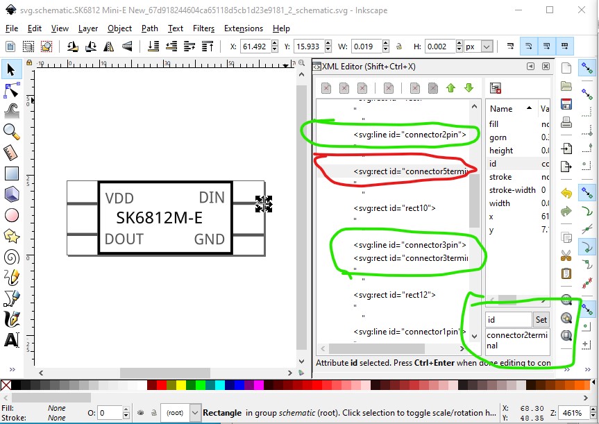
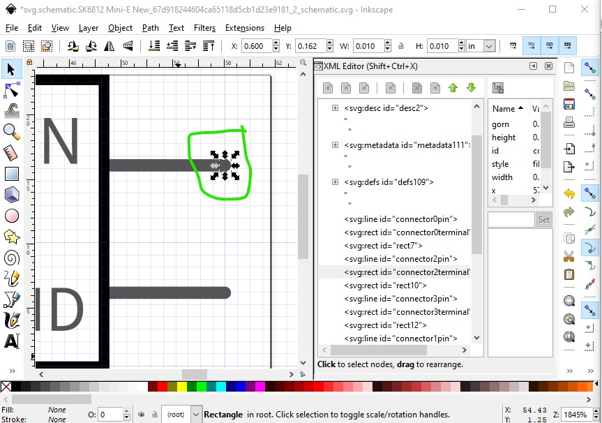
We see connector3 is now correct, so do the same to connector 0 whose terminal is named connector6. Then turn on the page grid (the grid is set to .1in on major lines, .01in on minor lines) and we see that schematic was mis aligned because the right hand pins are beyond the .1 in grid line.
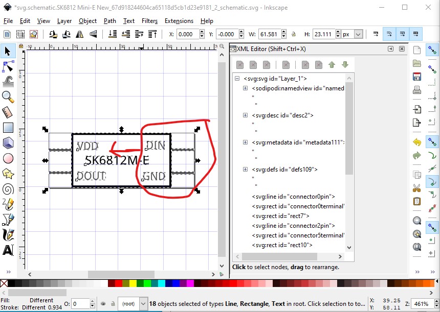
and thus need to move a bit to the left to align exactly to the grid.
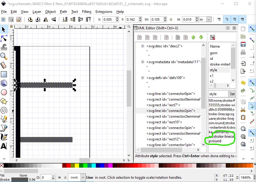
While I’m here I added a stroke-linecap:round to make the end of the lines round instead of square and changed the size and position of the terminal rectangle so it fits exactly on the .1in boundary and in the middle of the circular end cap on the line.
Then regrouped the entire image and set schematic as the group name and saved the file as plain svg. Now on to the fzp file to make sure all is well there. We need to remove copper0 from the entire .fzp file, starting with the layer definition:
<pcbView>
  <layers image="pcb/SK6812 Mini-E New_67d918244604ca65118d5cb1d23e9181_2_pcb.svg">
    <layer layerId="silkscreen"/>
    <layer layerId="copper1"/>
    <layer layerId="copper0"/>
  </layers>
</pcbView>
becomes
<pcbView>
  <layers image="pcb/SK6812 Mini-E New_67d918244604ca65118d5cb1d23e9181_2_pcb.svg">
    <layer layerId="silkscreen"/>
    <layer layerId="copper1"/>
  </layers>
</pcbView>
Then each connector definition needs copper0 removed
<pcbView>
      <p layer="copper1" svgId="connector0pin"/>
      <p layer="copper0" svgId="connector0pin"/>
    </pcbView>
becomes
<pcbView>
      <p layer="copper1" svgId="connector0pin"/>
    </pcbView>
  </views>
Now run the svgs through FritzingCheckPart.py to clean up and check for errors. Rezipped it to a new part and test

Schematic is now fine. The lines terminate correctly at the end of the pins, and the pins align to the .1in grid. Now on to pcb.

and pcb looks ok. It will only connect on the top layer (as the part is SMD.) Now to see if the gerber is happier.
No, still missing two of the pads. So back to the pcb svg to see why.

However copper bottom now shows no sign of the pads as it should

Well copper1 has a transform so lets start by trying to remove that.

to do so ungroup the entire svg (which usually removes transforms) and see what happens. It did indeed remove the transform, so lets see if that fixed the part. No cigar, still broken. That leaves us with something wrong about the path for the top two pads. So try duplicating and moving the bottom pads. Ungroup again because copying with groups will cause transforms. And success. There is something wrong either in Fritzing gerber processing (because pcb view is rendering the pads correctly) or the two paths. Duplicating and moving the bottom two pads to replace the top two pads makes things work.

We now have the missing pads in the gerber output. Here is the part that generated the above.
SK6812 Mini-E RGB LED-fixed.fzpz (12.0 KB)
Note you need to check the pads on pcb in this part to make sure they are the correct size because I changed px to in in Inkscape and the scale may be wrong depending on what dpi the original svg was in.
edit: Try this part with the ground fill and see if that cures the issue. If it doesn’t you may have hit a 0.9.6 bug as I remember someone else reporting a ground fill issue in 0.9.6 lately.
Peter
↧
Nrf24l01Adapter parts help please!

hello, I need this part for fritzing please help!
↧
Voltage reguletor and v&a meter

HELLO I WANT MAKE MY OWN POWER SUPPLY WİTH THİS PART BUT I NEED FRİTZİNG PART CAN YOU HELP ME PLEASE?
↧
↧
Volt & current meter part help

↧
Nrf24l01Adapter parts help please!
Welcome aboard! To my surprise we don’t appear to have one of these. A google search for “fritzing part nrf24l01 adapter module” doesn’t turn up anything appropriate. That may be because an Nrf24l01 will do in its place (the Nrf24101 is available in core parts.) To make a custom part we would need either a mechanical drawing of the board or at least a web site like this one with enough information to make one.
Peter
↧
Voltage reguletor and v&a meter
Not enough information here to identify this although it may be this part in core parts:

to find it enter rio rand in the search bar and hit enter. If you are making pcbs you need to check the footprint matches the part you have. Other wise again we would need a web site with the mechanical details of the part to make one.
Peter
↧
Volt & current meter part help
I don’t think one of these exists. There are voltmeter modules and ammeter modules but not the combined one that I can find. Again we would need a web site for the part you have (with a wiring diagram) to make a part.
edit: Instead of making a power supply, you may want to look at one of these
It takes up to 20V in (I use a laptop 20V wall wart) and is adjustable with a built in voltage and current display. There isn’t a Fritzing part (yet ) for them either but I will likely eventually make one.
Peter
↧
↧
Volt & current meter part help

↧
Voltage reguletor and v&a meter

↧
Nrf24l01Adapter parts help please!
As you know nrf24l01 need a 10-47uf capacitor between gnd and vcc so I use it ,and ther is some capacitor and resistor but I don’t know connections .And I am afraid of I haven’t got enough time,it is for a competition can you send .fzp file?
↧


