Looks good, except the left hand sketch again has a power/ground short on U49 this time. Corrected in this sketch.
accordion-left-hand-Sketch (5) (1) (4).fzz (177.3 KB)
Peter
Looks good, except the left hand sketch again has a power/ground short on U49 this time. Corrected in this sketch.
accordion-left-hand-Sketch (5) (1) (4).fzz (177.3 KB)
Peter
There doesn’t appear to be a footprint for this (it is an odd size and pitch). Since a full part isn’t that much harder than a footprint, here is a part.
Mpxv5004dp.fzpz (8.1 KB)
As always verify the footprint is correct against a real part before ordering boards.
Peter
FYI - I’ve been using NewHaven Display’s for several years. High quality, reliability. I purchase from them but they are on most electronics supply sites… they provide spec’s
That link explains why the original old part had a 16x4 BB pic and reversed LED polarity.

16x4 1604A LCD Display - v1 - 16x4 LCD display.fzpz (14.3 KB)
https://www.ebay.com.au/sch/i.html?_from=R40&_nkw=16x4+lcd+display&_sacat=0&_sop=15
OK, finally finished I hope. As always this was instructive as I hadn’t used eagle to fritzing before. I see a number of issues that need fixing, but I’m not likely to do them any time soon. By and large it does an amazing job, but it has a few issues. In any case here is the part, please report any errors you find.
msp432P401R.fzpz (48.7 KB)
Peter
Thank you so much. I will use it in the next couple days and note any errors I find
Thank you vanepp!!! I really appreciated your response and your improvement work. I worked a lot on the breadboard only, I tried unsuccessfully to install and use Inkscape with the correct font, ignoring everything else due to the little time I had available. I also apologize for not having responded and thanked you so far. I am happy with this collaboration. See you soon.
Oh, I only see now a little revision that you can do (if you want)… As I wrote, my font don’t work well… On the breadboard side, there are two labels on the main switch, in the lower left side, indicating ON and OFF position… they are in wrong small font.
Bye.
I just updated the file with the font size for on and off the same as the other font sizes.
Peter
The 16x2 didn’t have mounting holes in the PCB so I made a new part.

16x4 1602A LCD Display - v1 - 16x2 LCD display.fzpz (13.2 KB)
Datasheet - https://www.sparkfun.com/datasheets/LCD/ADM1602K-NSW-FBS-3.3v.pdf
Hi, I would like to use an SVG image as a logo for my PCB. I already created the SVG (on https://www.figma.com) and when I open the SVG file in the browser (Chrome) I can see the image correctly.
However, when I import the same SVG image on my PCB as a ‘Silkscreen Image’ on the top layer of my PCB the only thing I can see is a blacked out image

When I move the SVG to the bottom silkscreen of the PCB, I can see the image slightly
Is there an extra step I have to make to load the SVG correctly? Do I need to convert my SVG to a PNG file? If so, how can I keep the image quality?
Thanks in advance!
Sorry , I don`t understand exactly . can you tell me what exactly I have to do to update Program ?
The parts data base is a clone of this github repository:
to update it on Windows7 you need to do a git clone of this repository in to where you installed Fritzing in the Fritzing-parts directory (in my case
C:\fritzing\fritzing.0.9.3b.64.pc
in to directory Fritzing-parts)
once that is done you need to start Fritzing and then in breadboard view (or one of the others except welcome) click on Part->regenerate Parts Database and click OK. That will rebuild the database then exit Fritzing. When you restart Fritzing you will have the new parts database.
Peter
The link doesn’t lead me to an svg file. If you rename the svg file to .fzp (the forum often has troubles with svg files) and upload it here I’ll have a look at it. There are a variety of posts in the forum on logos (usually on copper rather than silk though) and it is picky about paths (I think the gerber code has bugs). Most of the people with expertise in this area are no longer active in the forums though.
edit:
Please upload the .fzz file of the board you want the logo in as well as the logo svg.
Peter
@vanepp thanks for your reply!
The SVG image: logo.fzp (2.8 KB)
The project file: ContactSensor ESP8266.fzz (216.1 KB)
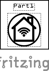
I don’t think you can do the logo as it stands. There is only one color in silkscreen. You are getting the black circle as the white circle under it all is changed to black. The rest of the outline disappears in the black of the bottom circle. You can print the white house and wifi bars as silkscreen which will be over the board color, but thats all. Silkscreen won’t do additive or subtractive layers as you have done in the svg. If you are good enough at path creation you can create a path that matches the black areas in the logo (as a single path) and use that as the silkscreen and that should work. I’m not that good at paths, so I did this instead (by deleting the circles and changing the path to black which Fritzing will do anyway) then adding a circle around the paths. This is constructed as a part because I thought I didn’t know how to properly format the svg (and I still may not) before discovering what the real problem was when I made it a part. I also shrank the scale of the svg to be somewhat compatible with the board as I don’t know how the load mechanism handles scaling. You may want to leave it as a part because I’m not sure you can move the logo around, it may be fixed in one place, a part you can drag around as you like.
logo.fzpz (2.6 KB)
You can load the fzpz file and it will put a part called logo in you mine parts bin. Dragging it in to pcb will give you the logo (and a part label that you need to hide by clicking on it and hitting hide.) Its size can be adjusted in the pcb svg for the part. Here is an image from pcb I have not hidden the part label in this one:
However it still needs work as gerber processing doesn’t like the path:
It isn’t worth pursuing at this point until I know what you want to do with the logo. It is entirely possible that converting this image (with the path corrected in some undefined manner, I usually move infliction points until gerber is happy, I think there is an overflow problem somewhere in gerber processing) will work with logo loading with a properly formatted svg (it needs 3 groups each with a copy of the image in it, labeled board, silkscreen and silkscreen0).
Peter
Thanks Peter .
my problem is Solve Completely by your Solution .
I hope be Good All Time 
@vanepp @opera_night thanks for your replies and detailed answers.
I changed the Silkscreen image so it loads a PNG file now, instead of an SVG file.

I have exported the PCB as a gerber project. If I open the gerber layers in some gerber viewer (Gerbv in this example) I can see the image in low resolution. How would this affect the actual PCB print, does anyone have any experience with that? I think the image is fine like this to send the PCB out for production, right?


