Quantcast
Channel: fritzing forum - Latest posts
Viewing all 31512 articles
Browse latest View live

Project ERROR: Easiest to copy the Boost library to ..., so that you have .../boost_1_xx_0

$
0
0

I’m unclear what you are trying to do here. Are you trying to build Fritzing from source (which is the only time you need to configure boost)? If so copy your copy of boost in to fritzing-app/src/lib/boost-xxx which is where the build expects to find it. If you just want to run Fritzing you should download the appropriate .zip file for your machine and install it (boost is included).

Peter


What did I do wrong with the PCB?

$
0
0

I’m trying to make a pi-hat PCB to a project I’m working on but after I load it to fritzing it shows up as a empty space… Custom SVG is here

Problems are:

  • It looks like it’s milling 2 times and just leaving the line.
  • Something weird with the solder mask to covering the copper?
  • Holes not being cut for the screws and the keep-out copper areas in the SVG isn’t there either?

What did I do wrong with the PCB?

$
0
0

Would you upload the sketch (the .fzz file) please? Upload is 7th icon from the left on the reply menu. At a quick look at the svg, it likely isn’t formatted correctly for a custom svg (although I’m not the expert on that either). Hopefully @opera_night who is much better at these will comment. This is usually tricky and hard to get right, although @opera_night has a number of posts on how to do it in the forum. The holes need to be dragged on to pcb layer from the pcb View section of core parts (the right hand window in Fritzing) or specified in the copper1/copper0 layers of a part. You likely want the first option here. I don’t think you can make them as part of the cutout custom svg (but I could be wrong). The keep-out is automatically generated from the parts, it isn’t a specifiable layer. There are tricks you can do with substituting mask layers from different gerbers to make odd mask requirements work, which involve generating a mask that does what you want (usually by removing something from the sketch) then coping the gerber it creates in to the real sketch’s mask gerber file.

Peter

What did I do wrong with the PCB?

$
0
0

Rather than repeating info I’ve previously posted, look at my most recent posts re making PCB’s.

the Upshot:
The PCB svg is not the same as a Part svg.
The PCB svg does not have copper layers.

I opened your file and recommend starting over as the time/effort to correct what you have will be inefficient.

Helpful (I hope) is screenshot of a basic PCB svg layer setup… Not important is the ‘compound’ shape (which is just a different word for a Path… Don’t fuss about that. What is important are the Layer names

If you redo it and need further help, having understood my post’s, we’ll have a common foundation of understanding to solve your problem.

And, yes, you can copy&paste elements from your current file into the correct layers in a redo (thus saving about two minutes of work…)

Lastly, the SVG can be made with a text editor (which is all an SVG is, a Text file). Thus, while most all drawing apps that export SVG’s are useable (to certain degrees), they can (and do) add stuff Fritzing can’t handle so, best to keep it simple. Especially for a First-Time. So, make a very basic PCB, after success, get to where you want to be in the next step’s…

[EDIT ADDED] If you’re trying to make a ‘Part’ (Parts have a PCB but, not the Board’s PCB) take a look at most any Part. For ref, here’s my microSDcard part as an example (and Peter has posted many helpful parts to look at) http://forum.fritzing.org/t/micro-sdcard-part/5866/4

SD reader, turn which way?

$
0
0

Hi guys

This is probably a stupid question - but I can’t seem to understand which way I should turn this SD card reader (Sparkfun SD card) in order to have it face the edge of the PCB, where I want to insert my SD card :slight_smile:

SDsd_2

Thanks!

SD reader, turn which way?

$
0
0

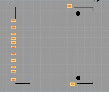
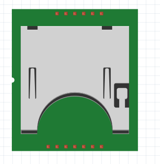
The only stupid question is the one you don’t ask … That said in pcb view the half round slot is on the edge where the U2 is (so right side of the picture above) with the 2 square and two round mounting holes. Breadboard view would need to rotate 90 degrees counter clockwise to match. The connectors are on the back edge of the card opposite of where the sd card inserts. In addition this assumes that the SD card is mounted on the top of the board, if you select bottom of the board (in the first line called pcb layer in inspector with the part selected in pcb view) it will change sides as oriented. Often the SD card is mounted on the bottom of the pcb especially on displays. Since a picture is worth a thousand words:

breadboard view

equivalent pcb view (rotated to be correct from the defaults)

Peter

What did I do wrong with the PCB?

$
0
0

Thanks, I redid the design in Illustrator instead of importing a SVG from my cad program and that seems to have solved it!
Just a couple more small things
According to the pi-hat specifications:
image
I’m not sure if it’s possible to define the soldermask in Fritzing at all, since I can’t add a copper layer in the pcb file I’m not sure how to correct it?

Second problem is the GPIO location, this is where it should be according to the specs:
image
(white box on pcb below)
But when I align the holes on the RPI and the custom PCB it looks like the gpio header is a bit off on the render below.


What did I do wrong with the PCB?

$
0
0

Regarding Soldermask:
Identify soldermask/ keep-out zones & other necessary features on a PCB drawing with clear text notes on requirements.

Regarding GPIO:
I think you’re on your own with this…
Consider that perhaps the part you’re using has an error/ or is another version…etc, graphics grid-size and grid snapping…


What did I do wrong with the PCB?

$
0
0

As before if you upload the .fzz file I’ll have a look at it and see if I can correct it.

Peter

What did I do wrong with the PCB?

What did I do wrong with the PCB?

$
0
0

Should have mentioned in previous post…

How you setup the lines/borders/stroke can create a similar issue - perhaps it’s the problem…

Generally, defaults are to use the Center of the lines but, they can be inner edge or, outer edge.

Example below shows a 20mm wide rectangle with a wide Stroke to aid seeing visual difference.
Top uses center of lines (meaning 20mm from Center to Center)
Middle uses Outer edge (meaning 20mm from Outer to Outer)
Bottom uses Inner edge (meaning 20mm from Inner to Inner)

What did I do wrong with the PCB?

$
0
0

The hole part of this is easy. As noted above, you can’t (AFAIK) drill holes from the board outline svg, you need to (as I did here) drag in a hole from core pcb view, change the radius to 3mm and then position it over the hole in the silkscreen. With the ring thickness set to 0 (as it is here) you will get a 3mm hole with no copper around it. If you want a copper ring, increase the ring thickness as desired (20 thou is the normal for pads) and that will add copper and create the necessary soldermask to leave bare copper. I suspect you are best off with a straight hole no copper though, so that is what I did. The board outline issue is more complex (and I’m less than expert at it). First, the PI3 part is an old 72 dpi part dimensioned in px (which causes scaling issues in Inkscape and sometimes Fritzing). Rescaling it properly indicates your svg matches the rescaled version so I left it alone. However the PI 3 part was overlaying the entire board making selection difficult at times (and probably adding extra silkscreen items we don’t necessarily want.) I fixed this by deleting the connector silkscreen in pcb3.svg (the board outline svg) as it was causing multiple copies of the image (offset by a bit) in the silkscreen. What little documentation there is suggests the path should repeat identically in the board layer and silk screen (I think this will produce silk lines around the board edge), but I did not do that here, just deleted the path for the connector silkscreen outline. Then I overlaid a 40 pin dual row header (which is broken in breadboard but not pcb) and did a “delete minus” on the PI 3 part and moved the connectors so they connected again (so the pads are green not red indicating no connection). That fixes up the connector outline in silkscreen which adjusting the pcb3.svg did not. Note that DRC (routing->Design Rules Check) fails on the between pad connections as it thinks there isn’t sufficient clearance. You may need to check with your board house to see if they can fabricate it (I think it is probably fine but it is worth checking). As the following gerbv output of the generated gerbers:

pcb3.svg with the connector outline removed. It looks to be there, it is just close to invisible, but if you click on the small dot on the line below and right click “save image as” you should get the svg.

Edit: Although it didn’t complain about not being able to render the svg, it also isn’t letting me download it. So here is the svg as an fzp file (so download the .fzp and change the prefix to .svg to get the svg!):

pcb3.fzp (3.2 KB)

and finally the corrected part which generated the gerbers above:

RPI_Telecine-hole.fzz (225.2 KB)

Peter

Fritzing 64Bit on Ubuntu 19.04 libssl error - program wouldn't start (Solved)

$
0
0

I fixed the problem manually, just writing my process down in case anyone else has the same problem.

Steps I took that resulted in the problem:

I downloaded the Ubuntu bit archive from Fritzing website, extracted to my local and ran ./Install and ./Fritzing

The error was “error while loading shared libraries: libssl.so.1.0.0: cannot open shared object file: No such file or directory”

What I expected should have happened instead:

Fritzing normal startup

My version of Fritzing and my operating system:

Fritzing 09b from Fritzing website
Ubuntu Studio 19.04

Please also attach any files that help explaining this problem
Don’t worry I fixed it!

So I got the missing libssl from Debian repo here: https://packages.debian.org/jessie/amd64/libssl1.0.0/download

Edit: run dpkg --install filename.deb after downloading it

It was not available through apt on Ubuntu 19.04 - I believe they have replaced this library with a newer one (most likely almost exactly the same thing with a new version number, so you could probably link it up)

If I am incorrect in my assumptions here please correct me. Anyway Fritzing is up and running again for me at least.

Futures discussion on github

$
0
0

what’s about the new 0.9.4 release?

What did I do wrong with the PCB?

$
0
0

Wow thanks! pure genius using a 40pin dual row instead of the rpi part… hated that it overlayed the pcb in the view all the time!

I noticed the DRC problem to but seeedstudio that I usually use can handle down to 4/4mil tracing so should be fine!

again, thanks a million for the help!


Futures discussion on github

$
0
0

It has been delayed a bit (I think mostly because the fixing up the website is absorbing a lot of time). There is a nightly built test version of 0.9.4 (which I am running) available on github somewhere. Unfortunately I downloaded and installed it without recording the url and now can’t find the reference to where it is on github. I’ll continue searching and post a url when (if?) I find it again.

Edit: after much head scratching, found it. It is in

“releases” (3rd icon from the left on the line starting commits) currently CD-288. If you click on that you will find the various flavors of the preview 0.9.4 release there ready for download. Note that so far (there is a proposal in to change this), this version uses the same user file directories as 09.3b so I’d advise keeping a backup of those two directories in case of problems (although I have been running 0.9.4 since early July without problems so far). It is in all of our interests to download and try this version and report bugs on github.

Peter

Request - Gikfun TEA5767 FM Stereo Radio Module

Request - Adafruit Buzzer 5V - Breadboard friendly

$
0
0

Does anyone have a Fritzing version of this part or know where I can find it?:

Thanks
-Wes

Request - Adafruit Buzzer 5V - Breadboard friendly

$
0
0

The usual answer is to do a google search of the form “fritzing part Adafruit 5V buzzer” and/or check the Adafruit fritzing parts repo on github. However there doesn’t appear to be such a part in either place, so I modified a buzzer part to create one with the correct .3 in spacing (at least according to the Adafruit page). As always if you are cutting a pcb verify the footprint before ordering boards.

adafruit5vbuzzer.fzpz (8.8 KB)

Peter

Futures discussion on github

$
0
0

Many thanks, Peter :+1:

I will… try to try :smiley:

Viewing all 31512 articles
Browse latest View live


<script src="https://jsc.adskeeper.com/r/s/rssing.com.1596347.js" async> </script>