With the warning I’m not a big board expert (I rarely make boards) here are some suggestions: I’m not real sure why DRC is complaining (I may have screwed something up in the part but I can’t see it.) I did reduce the traces on the ICs to 16mils. If you click on a trace and look in Inspector (bottom right window) you can set the trace size to a variety of standard values. I have done parts with much finer spacing than this for people (one was running close to the 8 thou minimum clearance of the usual board houses but the chip worked fine and the user even managed to hand solder it!) One thing I would probably suggest is dragging schematic out and routing it to make sure the schematic matches what you thing you have routed in pcb (it is awfully easy to make mistakes!) The board house will make what the gerber says. I don’t think there will be any problem with this, as nothing but the IC traces (and not all of them) are tripping DRC and the gerber output looks fine to me ) this is the two copper layers gerber output in gerbv:

There are a couple of things (non critical) on the layout as well. There are a couple or redundant vias (circled in red here), in general less vias is better (one less chance of a plating through failure causing problems.) The one on the bottom via on the bottom left can be removed by selecting the bottom trace and clicking move to bottom layer (as the bottom most part is through hole.) Pcb best practice is considered all traces horizontal or vertical, with bends at 45 degrees and straight in to connectors (with a bend a bit out from the connector if required.) but this actually only matters at RF type frequencies and isn’t likely to be an issue here I don’t think. The blue wire on this image will eliminate one of the vias by routing the blue trace on the bottom layer to the pin on the header to a via on the blue wire by the IC (changing two vias in to one)

And here is a copy of your sketch with the IC traces reduced to 16 thou:
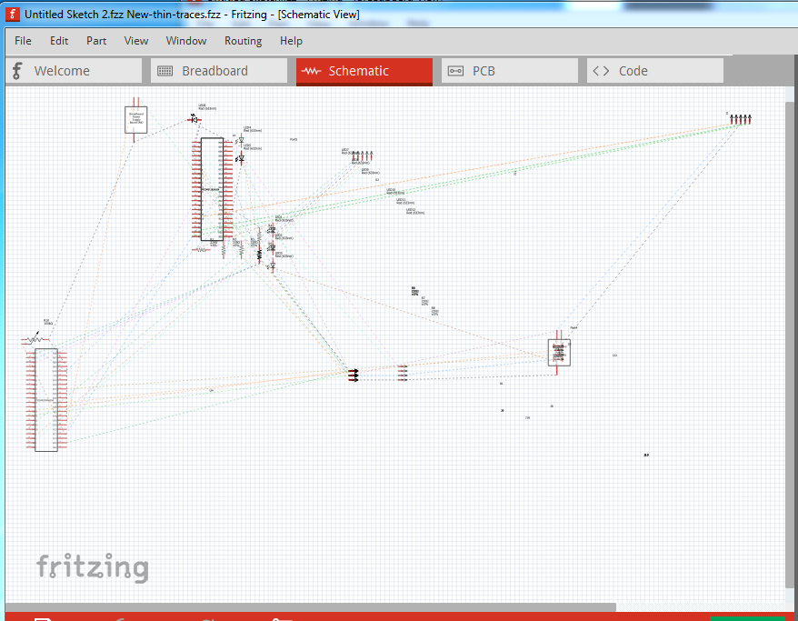
Untitled Sketch 2.fzz New-thin-traces.fzz (60.0 KB)
Peter


 .) The part however is broken in schematic and pcb (the red squares indicate undefined connectors.) I’ll try and fix it up in to a proper part and post it.