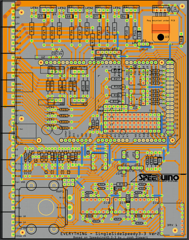
I guess you want to organise the placement of parts in PCB.
Spread the parts out and put ICs in the middle, because it connects on all sides, and click on a pad and all the connected pads will turn yellow. Best to keep connected stuff together. You put inputs and outputs on the outside, either together or opposite sides. Things in rows, groups, etc look more professional.
There is no perfect way to do it, so it just shuffling parts and manually routing.
