Quantcast
Channel: fritzing forum - Latest posts
Viewing all 28585 articles
Browse latest View live

Fritzing2Web - looking for contributors

$
0
0

Ater reading a lot about node and yarn, I managed to run it using your step plus extra thing:

1. Install Make for Windows: http://gnuwin32.sourceforge.net/packages/make.htm
2. Set up command alias using: DOSKEY make="C:\Program Files (x86)\GnuWin32\bin\make.exe" $*
3. Install Node plus npm.
4. Open with git bash the cloned repository and type: npm install eslint --save-dev
5. Run make test

What I got:

PASS test\index.test.js (6.985s)
  ApiClient getFzps
    √ Status 200 (750ms)
  ApiClient getFzpsCore
    √ Status 200 (359ms)
  ApiClient getFzpsObsolete
    √ Status 200 (266ms)
  ApiClient getFzp
    √ Status 200 (375ms)
    √ Status 404 (281ms)
  ApiClient getFzpCore
    √ Status 200 (406ms)
    √ Status 404 (313ms)
  ApiClient getFzpObsolete
    √ Status 200 (344ms)
    √ Status 404 (328ms)
  ApiClient getSvg
    √ Status 200 (344ms)
    √ Status 404 (265ms)
  ApiClient getSvgCore
    √ Status 200 (313ms)
    √ Status 404 (281ms)
  ApiClient getSvgObsolete
    √ Status 200 (328ms)
    √ Status 404 (359ms)
  ApiClient getFzbs
    √ Status 200 (454ms)

----------|----------|----------|----------|----------|-------------------|
File      |  % Stmts | % Branch |  % Funcs |  % Lines | Uncovered Line #s |
----------|----------|----------|----------|----------|-------------------|
All files |      100 |      100 |      100 |      100 |                   |
 index.js |      100 |      100 |      100 |      100 |                   |
----------|----------|----------|----------|----------|-------------------|
Test Suites: 1 passed, 1 total
Tests:       16 passed, 16 total
Snapshots:   0 total
Time:        8.381s
Ran all test suites.

Now make lint:

Got like 360 errors related to line breaks :smile: For this I typed make lint-fix as stated above by devs and it fixed it :smiley:

Now, I have no idea what should I do, I typed node src/index.js and nothing happens. Probably should find something similar like as http://fritzing.github.io/fritzing-parts/fzp/ somewhere? Help!


Inductive Charging set

$
0
0

I am looking to find an inductive charging set part, I need it rapidly for a project but I really don’t know how to create it myself.
Here are all the information about it : https://www.adafruit.com/product/1407

Has any of you already create it ? Or can anyone help me do so ??

Thank you

Inductive Charging set

$
0
0

Doesn’t look like there is a fritzing part for it. That said it depends on what you want/need from a part. It is pretty basic, just power in and power out. Two 2 pin headers (one for power in one for power out) might do. If you want a breadboard image that looks like the part that would be more complex. If you mostly need it for making a pcb I’d go with the 2 pin headers as that will give you the needed holes to either hook the wires in to or attach headers to plug the modules in.

Peter

Fritzing2Web - looking for contributors

$
0
0

You are a better man than I! Indeed those steps fixed it for me as well., well done. I’m also not sure what it should do at this point, as @sublimeartistry said earlier its possible this is only the api to access the parts repository and it won’t actually do anything (other than pass the tests) until the parts viewer repro is ready. Hopefully one of the developers may comment.

Edit: From the status 404 that we are both getting, I think there is a bad url to the repository and we aren’t getting the connection that we should (at least completely although it says all tests passed).

Peter

Fritzing2Web - looking for contributors

$
0
0

There are a few new repos in the Fritzing Github account and one that looks to be the base for the application that uses the API. It looks to have the capability to render the views and do a few other things.

GPON Fiber optic cabling simulation

$
0
0

I don’t know whether this is acutally possible.

I’d like to use Fritzing to simulate fiber optic cabling using PLC splitters.

to illustrate:
my laser light source has +3dB
1km single mode fiber has a loss of 1dB
a PLC splitter splits the light into multiple beams (1:2 / 1:4 / 1:8 / 1:16 — 1/128), each type has different loss. A 1:4 splitter for example has a loss of 7dB

I’d like to be able to see the current light strength at every point I click

[ OLS ] ----- (+3 dB) --------- [ 1km cable ] ----- (+2 dB) ------- [ PLC 1:4]
------ ( -5 dB) -------
------ ( -5 dB) -------------- [ 1km cable ] ----- (-6 dB) ------- [ 1km cable ] ----- (-7 dB) -----
------ ( -5 dB) -------

Is Fritzing the right software to do such a simulation?

Thanks

GPON Fiber optic cabling simulation

$
0
0

There is no sim, light or electronics, in FZ, just EDA

INK (GLCD) Display Part (NOKIA-5110)

$
0
0

These are useful, low-cost, low-thickness INK display’s with a Backlight.

I made three Variants of the connections:
• Variant 1 - Top Row
• Variant 2 - Bottom Row
• Variant 3 - Both Top & Bottom Rows with internal connections. Pads will be placed on the PCB - if you don’t want the pads for an un-needed row, use a different variant. Variant3 helps routing traces as needed without needing jumpers if they needed to crossover a trace.

I made these for my own use thus, regarding Fritzing Part ”Standard’s”: some were followed, others were not (particularly Font Size, Font Color and Line-Width).

Images of Variants along with an example in use…

Much thanks to ‘vanepp Leader’ for insight on Part Making.

Nokia 5110_INK_Display_BtmRow.fzpz (12.4 KB)
Nokia 5110_INK_Display_TopRow.fzpz (12.4 KB)
Nokia 5110_INK_Display_TwoRow.fzpz (17.2 KB)


GPON Fiber optic cabling simulation

$
0
0

Assuming you are trying to model the path power loss at each point I suspect a spreadsheet with a calculation for the accumulated loss at each point would do what you need. As Old_Grey said, Fritzing doesn’t have the tools to do this.

Peter

INK (GLCD) Display Part (NOKIA-5110)

$
0
0

Over all a nice job (I have a previous part from someone but I like yours better :slight_smile: ). These are a nice cheap display and there is a nice library available from Sparkfun. That said your part has a few issues (mostly in schematic, and mostly style, yours works just fine mostly). Both breadboard and schematic are lacking the correct layerIds. The only thing I know that affects is svg export of the part from Fritzing will fail. The holes in pcb should be labeled nonconn0-4, with a stroke-width of 0. This is secret Fritzing code that causes the gerber output to only put the hole in the drill file (yours will work but it puts copper on the copper layers which the drill will then drill out). I changed schematic to look like this (mine on the left yours on the right):
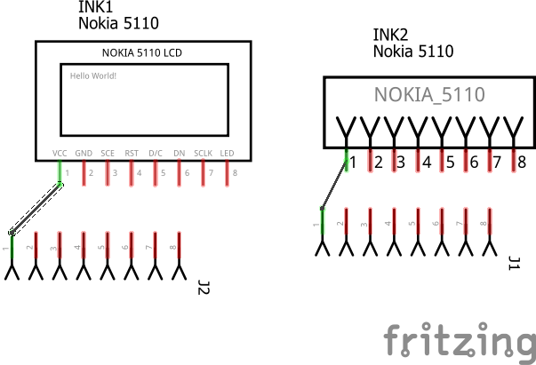
nokia_schem

The wire on yours connects to the middle of the pin (rather than the end as is desirable) because you don’t have a terminalId defined in the schematic svg. Without the terminalId the wire connects to the center of the .1 in long pin which isn’t what we want in this case. Below is a modified (with a new moduleId so you can load both parts at once) copy of your Nokia 5110_INK_Display_BtmRow.fzpz part with my changes (in addition I rescaled them all to the standard scale as well as fixed the layerIds).

Nokia 5110 INK Display_BtmRow.fzpz (7.3 KB)

Peter

In schematic diagram it shows there is some connection need to be routed

$
0
0

hello everyone, i am still new in fritzing, i have a problem with my schematic diagram, it stated that there are 12 of 15 routed - 6 connection still to be routed. I don’t understand this as my breadboard diagram shows that all has been completely routed.
Can someone help me with this?hc-05-serial-2.fzz (33.7 KB)

In schematic diagram it shows there is some connection need to be routed

$
0
0

You are going to have to fix that SCH first because there are parts miles away from the circuit. Bring those parts close to the Arduino, because they are so far away that I can’t see all of it at once due to it being microscopic.

EDIT
There is a lot more wrong than I thought.
I suggest going to SCH view, Routing/Select All Traces, then Edit/Delete.
Do the same in PCB view. You need to disconnect all solid connections in other views so they become ratsnest or you will destroy the sketch when you change connections in the primary view.
Now go to BB view and fix all the problems.
See the red TXD pin on HC-05, that is showing you it’s not connected.
Red pins on the UNO too.
N trans is not in BB, ie red dots
Pin 7 of L293D is not connected to yellow wire. Click on pin 7 and you will see no junctions on the yellow wire turn yellow, just the row on the BB
Red bendpoints on yellow wire not connected.

Check the whole thing for red pins, and click on green pins to follow connections to make sure it’s definitely connected. Remember if things are touching it doesn’t mean anything is actually connected, it’s like all EDAs there is no snap connect for touching stuff.

Df robot ph sensor

$
0
0

Thanks a lot! But that is just one part can i ask you for the sensor part too?

Thank you in advance
Nicola

In schematic diagram it shows there is some connection need to be routed

$
0
0

thank you sir for helping me out, I am trying to do as what you’re suggested.
with deleting the solid connections, makes me ease the work at least (less mess) , and I want to ask, If I need to do correction of the SCH so I have to do the same correction on PCB?

In schematic diagram it shows there is some connection need to be routed

$
0
0

You need the BB view perfect first, and if you try to fix it without deleting all the solid traces in the other views it will corrupt the sketch and you will have to throw it away because it will be impossible to fix.

After you fix BB view - you can post it again for checking - do the next view and trust the ratsnests. You can click on a pin and everything connected will turn yellow, and that might give you an idea of a shorter route. If you need a junction put a bendpoint on the trace and run a trace to it - hold ALT and click and drag a trace to the pin -. Always grab junctions and move them to make sure traces stay connected.


INK (GLCD) Display Part (NOKIA-5110)

$
0
0

Peter, Thanks for the comments…

Regarding the re-name of Holes to “nonconn”. Agree and started to do it (as shown on PCB in screenshot).

Regarding the Schematic - graphic: Was torn between similar to yours and what I ended up with. Preferred mine for economy of size. Also, as mentioned in my write-up in post; the fonts are not as Fritzing wants (my eyes are 70yrs old and cannot see the light gray tiny fonts).
[Also, not mentioned - For the Two-Row Version,I chose to sequentially number the pins rather than duplicate them as that’s how I wired my hardware.]

Regarding the Wire connects on the terminals. Agree (though I left them as-is because it seems many/most of the parts I use also connect at the center. But, at the end of the terminal makes much more sense and will change them).

Scaling? Why did you rescale them and what was wrong with the scale? My Inkscape is set to Inches and the default of 96px/inch.

Really, really weird! Re-Opening the files in Inkscape:

Hole stroke-width: they were set to 0 but, reopening the files shows them at 0.01

Lacking correct ID’s… even more weird - you can see in the image that all ID’s and Layer names are set to what I believe is correct. So, I’m, either not sure of what you’re referring to or, something software-wise is happening???

You mention an SVG issue if exporting from Fritzing will ‘Fail’: The files I posted were Exported from Fritzing so, if you were able to open them, and, indeed check-out the part, well, I’m further puzzled…

I see your files are nicely flowed and you must have manually re-arranged/re-flowed them - did you do it in an editor? Perhaps your editor removed the ID’s ( I’ve noticed that Inkscape sometimes does a re-naming if it doesn’t like an ID or is duplicated or it’s contents have changed. FYI - I use a Mac.

In schematic diagram it shows there is some connection need to be routed

$
0
0

I have done for the BB view, but I don’t quite sure it is right or not. It looks correct ahaha, but could you please check my battery connection and the I am not sure in connecting 5V and Vin in arduino, because I am using the 9V and 3V of dc battery.hc-05-serial-2.fzz (26.1 KB)

In schematic diagram it shows there is some connection need to be routed

$
0
0

I’m not very good at knowing if that actual circuit will work, so unless you tested it working someone else will have to look at it.

In BB I like to make sure it looks very clear so people can’t make mistakes. It’s not critical because I think it’s ok, but little things like :-
The diode near the button looks like it’s not touching the hole when it’s connected to the hole under.
I would move the N trans up 1 so you can see the leg and blue wire are actually. I like pin and wire on separate holes and not on top of each other.
I also tend to not run wire over BB holes but between so there is no chance of something connected by accident. Things like the white wire near the resistors.

Possible errors are
red wire near #15 on BB not going anywhere
I don’t think you can put 2 wires in the same header hole on the UNO

Some hints

INK (GLCD) Display Part (NOKIA-5110)

$
0
0

[Rather than updating my last post, I’m doing via a Reply]

I updated/changed my files to reflect:
• All file’s:
Changed Hole Stroke-Width=0

• Schematic’s
• Terminal End connections
• Changed graphic to Box with single-lines (not Y )
• Changed sequential numbering to Duplicated 0-8

• PCB’s
• Holes: changed ID to ‘noconn’

As said/shown in previous post, all files have correct layer names and ID’s. I opened them in several different editors (xCode, BBedit, eclipseNeon, OpenOffice, TextEditor) all show ID’s correctly.

Exported them from Fritzing.

I think the only remaining thing for me to understand/change are the ‘Scaling’ you referred to… However, given that, in Inkscape, 96px = 1inch, logic suggest scaling them by 1.0427. Rather than rescaling for these re-posted parts for you review, I’ll wait for clarification of ‘scale’…
And, any ID’s that you mentioned where I may be missing a point you’re making (sorry, old and slow).

Thanks again
Nokia 5110 INK Display_v1.fzpz (12.0 KB)
Nokia 5110 INK Display_v2.fzpz (11.9 KB)
Nokia 5110 INK Display_v3.fzpz (13.6 KB)

INK (GLCD) Display Part (NOKIA-5110)

$
0
0

As always, your part your choice :slight_smile: I prefer my version and prefer (in case of later mods) to have the text as text elements so later changes are easier but your method certainly works as well (it is just more complex if you want to make changes later as you have to delete the path and redo the text).

The parts format document calls for the viewbox to be set to 1px = 1 thou inch (which at 96dpi in Inkscape is a scale of 10.41667 in the document properties page. That also makes setting the hole size in the xml easier so I generally do it. It won’t affect operation as long as the height/width are set in either inches or mm so Fritzing knows the real size of the document. If the default px (and no units defaults to px) is used Fritzing will make a guess as to what the dpi was (72 for old illustrator, 90 or 96 for older/current versions of Inkscape) and sometimes gets it wrong and causes scaling issues in parts.

What can I say? :slight_smile: Inkscape does odd things sometimes (but I’m far from an expert on svg editing so there may be a good reason for it). I think it converts to some high resolution internal number representation and sometimes has round off effects. That said when I reopen the pcb svg on Windows in Inkscape the stroke-width value is still 0 as I expect.

The breadboard svg is actually a copy of the pcb (as is icon). Schematic is really schematic but is partially wrong in that there should be only one group for the entire document and it should have the label schematic not silkscreen (which is only used in pcb) or what ever is in the fzp file (which will usually be “schematic”) in the layerId line. From your Btm_row part above the fzp file has:

  <schematicView>
   <layers image="schematic/Nokia_5110_btm_3f8387282d7ce92c6d9b0502a0db1f25_1_schematic.svg">
    <layer layerId="schematic"/>
   </layers>
  </schematicView>

meaning the group currently set as “silkscreen” should be “schematic” (which is somewhat below it as another group). Same with breadboard and icon, there should be a single group for the whole drawing with the id “breadboard” (which is set in the fzp file as well). Icon is typically a copy of the breadboard svg, and Fritzing doesn’t seem to care that it isn’t called “icon” as specified in the fzp file. I suspect (but haven’t tried) that the text in group silkscreen will be omitted from the part during an svg export.

I wasn’t quite clear enough, the part exports and works in Fritzing just fine with incorrect layerIds. However if you put the part in a sketch and then do a file->export->as image->svg of one of the views when a part has has an incorrect layerId, that part won’t be in the resulting svg but the other parts (with a correct layerId) will. It is fairly minor but annoying because it causes questions when someone uses such a part in a sketch and then asks why the part doesn’t show up on svg export.

The formatting is a result of two things: I ungrouped all the svgs (which removes transforms and unneeded groups that the Fritzing exported likes to add and then ran it through my parts checking python script which converts silkscreen color to black (to show up in Inkscape), converts style commands to inline xml (because sometimes Fritzing won’t deal correctly with style commands in all cases and inline is equivelent) and removes the trailing px from font-size statements which Inkscape puts in because CSS requires it, but which breaks Fritzing (as it converts font-size with a trailing px in to a 0 font-size but only on export). As part of checking the part the input formatting is lost so the script finally runs the xml through a pretty printer which is what gives the clean output (until Fritzing’s exporter adds the groups again.) Hope this helps! Parts making is complex and poorly documented, so we tend to learn as we go.

Peter

Viewing all 28585 articles
Browse latest View live


<script src="https://jsc.adskeeper.com/r/s/rssing.com.1596347.js" async> </script>