Quantcast
Channel: fritzing forum - Latest posts
Viewing all 28589 articles
Browse latest View live

INK (GLCD) Display Part (NOKIA-5110)

$
0
0

Just saw your post after I posted…

Yeah, clearer documentation would be helpful and would eliminate back-and-forth exchanges. Thanks for hanging with me on this!

Yes, in first group of parts I did use the ‘Reuse’ feature for some items - guess that’s not a good idea. The files I just posted do not reuse files.

I’ll review your recent post and update as needed (however, it’s unlikely I’ll change the font size BUT, I will change the text Path’s to Text (paths also make a hassle to edit the text…).

Thanks!


INK (GLCD) Display Part (NOKIA-5110)

$
0
0

Happy to help, lots of folks helped me when I started a couple of years ago. In theory (but I’m not sure about practice) Fritzing will only take ocra and droid sans fonts and anything else needs to be converted to a path. That said I think I have seen examples of text in other fonts that Fritzing rendered. I’d suggest trying a test case before doing a large conversion to make sure Fritzing will accept and render another font.

Peter

In schematic diagram it shows there is some connection need to be routed

$
0
0

This doesn’t look correct, but I’m not sure what should be happening. Is the 9V battery powering the Arduino (alternatives would be a wall wart connected to the arduino power plug or a USB cable plugged in). If so the +9V side needs to go to Vin and that 9V will be reduced to provide 5V and 3.3V on those pins. Both the 9V battery and the 3V (12V as the note says?) batteries appear to be connected wrong. I’d expect the - side of both batteries to go to ground (which by the way should have black wires usually). The +9V wire should go to arduino vin and the 3v/12v battery + should likely go to the motors. The diodes across the motor will likely mean that the motor will only go one direction (the other direction will likely short the motor driver). Usually motor drivers have internal protection diodes but you would need to check the data sheet to see if that is true here. What connects to the power plug on the bottom?

Peter

INK (GLCD) Display Part (NOKIA-5110)

$
0
0

I opened your file in BBedit so I could more clearly see what’s going on. Real simple!!!
It turns out that the Fritzing documentation I read regarding building a part is so bad and correlates very little with what you did.

Before starting out, I reviewed the doc’s and did outlines of ICON,PCB,Schematic and BreadBoard files per the doc’s. Wasted a lot of time - guess the learning was worth it but, not a good representation of Fritzing…

The doc’s call for different organization structure which led me to most of the problems. But, now, with your help and clarity from your file, I see the light… and it really is simple.

FYI - Two of your files changed the pads from Circles to Ellipse’s. That happens in Inkscape if just breathing on a Circle.

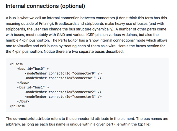
The doc’s call for sub-level grouping of connectors if they’re part of a buss (as in the TwoRow version). That’s how I did that version. But, now that I see how different your file structure’s are, I wonder if the Buss is even necessary since the editor panels have an Interconnect feature… ?

I’ve used both OCRA and Droid-Sans for part&pcb and that font is good for me (just can’t use a tiny size or light grey)…

I understand the scaling requirement.

INK (GLCD) Display Part (NOKIA-5110)

$
0
0

That is likely an artifact of the rescaling (possibly due to rounding). After a rescale circles are often an ellipse with an rx and ry rather than an r. My script looks for that in the pcb svg (but not the others) and flags it as an error because the gerber output won’t create a hole for an ellipse. In breadboard or schematic it usually isn’t an issue.

I’ve not seen that documentation, it may be for an older version (much of the documentation around is). All I’ve ever used for buses is a bus definition in the fzp file which defines the bus name and specifies which connectors are in this particular bus. The check script checks to make sure the connectors exist in the svg, but I’ve never had to put them in a special group (and the current parts file format document doesn’t specify any groups needed) and usually leave them in the layerId group. The new parts editor internal connection feature creates the necessary buss definitions in the fzp file. If (as in this case) the pins are connected together internally to the board, then they should be bussed in the fzp (or via parts editor) so the nets come out correctly.

Peter

Df robot ph sensor

$
0
0

That will be somewhat more difficult. There don’t appear to be any specs about size etc. around and it doesn’t have any connections that Fritzing needs (it connects to the interface board which connects to Fritzing). If you can get a jpg or png image of the sensor (there seem to be a few around on the net) it may be possible to convert the jpg or png to an svg and add it to breadboard but I at least have never had any success doing so. Alternately someone good at making graphic images (which again isn’t me :slight_smile: ) may be able to create an svg that looks enough like the sensor from the images available to do what you need.
Peter

INK (GLCD) Display Part (NOKIA-5110)

Df robot ph sensor

$
0
0

Can be done after checking this link. It has the probe size and also a good png made from some .svg drawning.


INK (GLCD) Display Part (NOKIA-5110)

$
0
0

If you are thinking that the “bus0” and “bus1” ids need to exist as groups in the svg, then yes you have misunderstood. They only need to exist (and be unique) in the fzp file and connector0, connector1, connector2 and connector3 need to exist in the fzp file and contain a pin svgId definition such as svgId=“connector0pin” that exists in all the svgs and everything is happy. The bus definition stuff is only in the fzp file.

Peter

INK (GLCD) Display Part (NOKIA-5110)

$
0
0

Yes, it is for the fzp metafile… It’s all clear now.
Thanks

DRC Overlapping problems with QFN / SMT

$
0
0

Hi!

I have a custom made part for the MPU9250 9-axis motion sensor. It is a 3mm 24-QFN package, so quite small.
Additionally I use a Decawave DWM1001, which is - kind of - SMT package.
See the datasheet: https://www.decawave.com/sites/default/files/dwm1001_datasheet.pdf
The MPU9250s pads are some 0.18mm, the DWM1001’s pads are 0.35mm apart.

Below are 2 images showing the details of the 2 elements (DWM1001 only right half):

For both MPU and DWM I get DRC overlapping errors for every pad that has a connected trace and their neighboring pads - Why? It doesn’t matter how thin I set the traces.

DRC Overlapping problems with QFN / SMT

$
0
0

The DRC error basically tells you a human eye needs to check them because there might be contact. If you can see gaps and the gap is wide enough for min width manufacture - I think it’s 0.006"(0.15mm) for most houses - it should be ok. You can print it out an check.

That being said, where did the part come from. Like is it made properly. I’m see orange traces with red spots, and that means the bottom layer copper is close, which is weird when a SMD only has a top layer. Is this a double loaded PCB.

DRC Overlapping problems with QFN / SMT

$
0
0

Hi!

Thanks for the hints!
It is a double layered PCB with the MPU9250 on top and the DWM1001 on the bottom side. Both are custom made parts by myself. Could it be a faulty SVG?

In schematic diagram it shows there is some connection need to be routed

$
0
0

I was planning to run my device with external 12V dc battery and also I want to make it rechargeable too , so I guess I need to add ac adapter socket and its charger but i can’t find reference on it. I also have difficulties in connecting the 9v battery and 3V battery in series (I found one source of someone tried to connected like this but when I tried, it is not connected to the 3V)

Code for sk9822 fast led


DRC Overlapping problems with QFN / SMT

$
0
0

If the IC foot print is only on one side they should be ok, it’s just that I thought there might be an error in that part where pads were on both sides.

The usual procedure is to print it out an check parts fit on it, because you don’t want to get it made and find out it’s wrong.

DRC Overlapping problems with QFN / SMT

$
0
0

I have found that Fritzing does not deal well with individual parts that have tight spacing when checking with the the DRC tool. It almost seems that it ignores the settings and uses the default spacing when checking between pads on a single footprint. All I have done is made sure it looked exactly as I intended before sending them off to have manufactured.

What you will find when you get the boards back from your manufacturer is that the spacing is so tight that you will not get any solder resist between the pads but otherwise they will be exactly what you have designed.

Castellated Hole

$
0
0

Hello all,
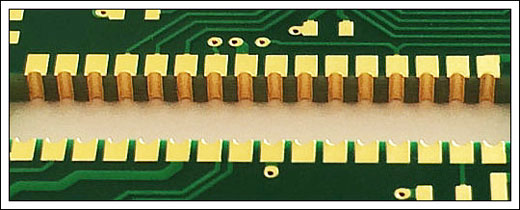
I wanted to make a PCB to mount on another PCB. For that I wanted to use castellated holes. Is there any way to do this in fritzing ?
Thanks

This is what I am talking about-20160527155822_760

Castellated Hole

$
0
0

I am not aware of anyway you can do this in Fritzing because Fritzing does not allow holes to intersect the edge.

The place I have make my boards charges an extra $15 for them so I have never bothered to figure out how to do it since that is more than 3 times the cost of the PCBs at $4.90 for 5@ 100mmx100mm. I usually just make finger joints (same as the castellated but with vias connecting both sides and not right at the edge) and they are easy to solder you just have to make sure you get some solder under them like soldering a QFN package.

If you must have them castellated I can think of two ways.

  1. (this one will work for sure) Make your boards a little larger than needed and then cut the edge off yourself. I have done this with Arduino Pro Minis to mount them easily on custom PCBs.

  2. (up to your board shop if they will do this) First you create your PCB larger then needed to ensure the holes are exported during Gerber export (check with a gerber viewer like Gerbv). Once you have them exporting correctly and have saved the gerbers you would reduce the size of the PCB in Fritzing until it cuts off the holes and then export the gerbers again and use the drill layer ( and possibly the copper layers if they are not complete on the second export) from the first export with the other layers from this export. That should give you a set of files capable of creating a castellated PCB.

There is a discussion about how to create a castellated board on stack exchange that you may feel like reading.

In schematic diagram it shows there is some connection need to be routed

$
0
0

Ah, that explains a few things! Indeed you have a number of problems and as it stands you are likely to blow up the Arduino. Your problem with the batteries is a Fritzing quirk, the bendable leads on the battery are both female and thus won’t connect to each other. You need to run the wires from the positive of the 9V battery to an empty row on the breadboard and then connect the negative wire from the 3v battery to the same row on the breadboard to actually get a connection (this is why schematic shows the batteries to be unconnected to each other). Your current connection would work in real life but not of Fritzing. Alternately you could use only the 9V battery and note that it is in real life a 12V battery. Now the negative side of the battery wants to go to ground and the positive side of the battery wants to go to Vin on the arduino (I recall checking the schematic for the arduino once and deciding that you could power Vin from there if you didn’t use the USB connector or the barrel jack on the Arduino but you may want to verify that). The Vin connection (expecting 9 to 12V in) feeds voltage regulators on the Arduino that provide 5V and 3.3V out to the pins labeled that. You are attempting to put 12V on the 5V output to the Arduino which is likely t blow the board. If your motors want to run from 12V (which is likely, the Arduino regulator can only supply a limited amount of current at 5V and likely won’t run the motors successfully) they too would need to connect to the battery positive or the Vin pin. Motor U4 is connected wrong. It should connect to the motor output on the LM293 not the IO pin on the arduino (which doen’t have the capacity to drive a motor and would probably damage the Arduino). I’m unclear what the transistors and diodes are supposed to do, but I don’t think it is correct. As noted before the motor driver probably has appropriate back emf protection but you would need to verify that (a quick look at the data sheet indicates that is correct). In your current configuration the motors will only go one direction (which may be what you want), to go both directions you would need to use two drivers per motor (i.e. one l293d will only drive 2 motors bidirectionally). I don’t think you need either the transistors or the diodes. Hope this helps some.

Peter

Viewing all 28589 articles
Browse latest View live


<script src="https://jsc.adskeeper.com/r/s/rssing.com.1596347.js" async> </script>