I have made the original sketch which I sent you originally it is how I have my circuit currently set up. It is good to have because I know that everything is working with this circuit. I know you have helped me greatly, and suggested some changes that could be beneficial but I’m not sure with which circuit I am going with. If I’m honest I don’t want to be moving parts now when everything is working as it should be. It’s took me just over a year and a half to get this project somewhere close to the end. I just need to move onto the pcb now and then I can get everything cased. I have started to attempt the pcb view but it is a mess but everything is routed. Please would you check my drawing and the connections on it? I think the pixel strip isn’t correct in the schematic view. Thank you for your helpChewie original circuit.fzz (156.0 KB)
↧
Schematic to breadboard layout
↧
Schematic to breadboard layout
Yep, you look to have moved the neo pixel in schematic and that broke the +5V connection (the end of the wire going to the neo pixel doesn’t connect to anything. As well the 6n138 is incorrect wired in breadboard. The chip needs to be rotated 180 degrees (the current one is the correct direction for an IC which is wrong in this case). To fix that I deleted all wires connecting to the 6n137 in schematic and pcb then in breadboard clicked on the 6n137 and rotated it 180 degrees. That gets the pins in the correct place for your working circuit. As well the wire in breadboard on din pin 5 was in the incorrect place. It should go to pin 3 not pin 4 (which is nc). I also moved a couple of the wires in breadboard so there weren’t two connections on one pin (which won’t work on the real breadboard) but they are cosmetic. With those corrected you should now have a working copy of the original circuit as it is on the breadboard. here (I didn’t finish pcb however). PCB looks somewhat OK as far as routing goes, but a few suggestions:
-
Board houses charge by the square inch, so a bigger board is more expensive. In this case I’d probably mount the mega on its own (to save board space) and run jumpers or perhaps fit the circuitry in to a mega shield format and put your parts in the shield (to save the cost of the space for the mega on the board). As well you want to group the components as close together as possible (with still being able to route the traces) to minimize the cost of the board. Note if you are putting the board in an enclosure, you need to be mindful of the dimensions of the enclosure and add holes to the pcb to allow it to be screwed in to the enclosure.
-
currently the pot over lays the neopixel which you probably don’t want in practice. In fact probably the neo pixels want to go to header connectors because I would guess they will be somewhere remote from the board.
-
The usual advise for pcb routing is horizontal and vertical traces with no right angle corners (bends should be at 45 degrees). This mostly mattes in RF circuits and right angle connections would work fine here.
-
As noted the neo pixels take high current so their power leads should be separate from the power leads to the rest of the circuitry and be as wide as possible (to increase their current carrying capacity. I would actually not put the power wires on the board at all but run a large gauge wires from the power supply to the ground and +5V pins on the neo pixels. In all you look to be doing pretty good
 .
.
Chewie original circuit_fixed.fzz (157.1 KB)
Peter
↧
↧
Creating Ground Vias
Can you generate ground fill without automatically generating those randomly placed ground vias?
↧
Schematic to breadboard layout
Thank you for taking time to look at my circuit and fixing it. I did indeed move the pixel strip in the schematic view. Because I noticed the pins were green but the ground wasn’t. So I moved it and the lines appeared but the ground pin still isn’t connected. Is that right? because I have the ground pin connected into ground on my breadboard. Thank you for the advice I will try and keep my traces horizontal and vertical with 45 degree angle connections. I have an idea the size of my enclosure will be, but not exact yet. I am going to try and make it as a shield for the mega. The reason why I have my pixel ring on top of my pot is because that is how the final design is going to be. the pot will go through the pixel ring. But I think I am going to connect them by using wires from the pcb.
I’m sorry I don’t fully understand what you mean with point 4.
As noted the neo pixels take high current so their power leads should be separate from the power leads to the rest of the circuitry and be as wide as possible (to increase their current carrying capacity. I would actually not put the power wires on the board at all but run a large gauge wires from the power supply to the ground and +5V pins on the neo pixels. In all you look to be doing pretty good
.
↧
Creating Ground Vias
It will not create any vias on its own. Odds are what you are seeing is vias you have used during routing being blended in to the ground plane.
↧
↧
Creating Ground Vias
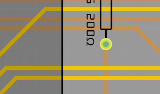
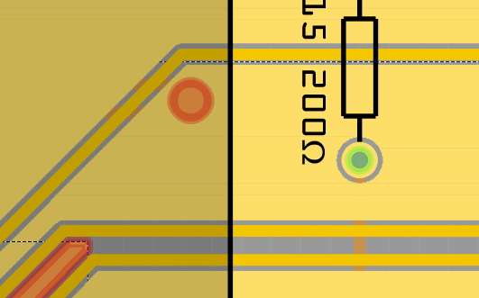
Maybe, but I haven’t added any vias that I’m not using, and I do all the routing manually. See attachments - one with the ground fill shows a via, but when I remove the ground fill it’s gone.
↧
Schematic to breadboard layout
Moving the part is one way to correct that problem, but you then need to check all the connections on the part to make sure they are all connected (in this case they weren’t which caused the problem). I expect the +5V connection to the neo pixel was not actually connected to the neo pixel in the original sketch. When you moved the neo pixel because +5V wasn’t connected that connection didn’t move with the neo pixel (because Fritzing didn’t know it should connect there) leaving the +5V connection unconnected with the wire hanging in space (and that in turn reflects in to breadboard and schematic view potentially causing problems there as well). Worse, if that dangling wire contacts a pin on the neo pixel (which it didn’t in this case) it will make a connection there where you don’t want one. If you put the cursor on the pin of a part (for example the +5V pin on the left of the top neo pixel) and left click the mouse button all connections will highlight in yellow. In the example the +5V wire on the neopixel, the T that denotes the +5V net and the +side of the capacitor all turn yellow indicating that these three points are connected together as they should be. After moving a part you should check all the pins to make sure that the connections all still go where they are supposed to. If you try the same thing on your Chewie original circuit.fzz you will see that the schematic looks (and is) incorrect, although it is not quite as incorrect as it first looks (likely a Fritzing bug here). If you left click on the ground pin the - terminal of the cap, the ground pin and the ground pin of the neopixel all light up yellow indicating a connection, even though on the screen the ground wire to the neopixel ends below the neopixel and does not appear to connect. Same with the di pin, while it appears on the screen to connect on or near neopixel ground, it really is on di. Selecting the neo pixel and moving it slightly causes the screen to update correctly showing the di and ground connections (with ugly wire layout) and the +5V neo pixel unconnected which is what pcb view is showing. I usually prefer to lock the parts in place and either move the wires til I get a correct connection or delete the wire and rerun it to get a connection. The click to highlight the connections to this net (which works in all views) is a very useful tool for insuring you have all the connections you expected to. It is how I find these errors when a sketch is doing something unexpected.
Ah! now it makes sense. Either method (mounted on the pcb or connected via wires to the pcb) should work as long as the pot selected will fit inside the neo pixel ring (I assume there is a hole in the center of the ring). Then which ever method is easier mechanically is what you should do. If the enclosure has a lid where your board and the mega under your board can connect with the neo pixels the jacks and the pot will all come out one plate that should work (although it depends on the position of the holes in the enclosure plate exactly matching position on the pcb which can be a pain to do, with wires to the board the enclosure holes are independent of the panel hole dimensions as wires will bend unlike neo pixels or jacks soldered to a pcb  . I usually opt to use wires to make my life easier but either will work.
The issue with the power wiring to the neo pixels is voltage drop at high current. The neo pixels sometimes when many or all the leds are on and the clocks align (which will be only sometimes) draw a lot of current. That current in turn causes voltage drop in either the wires or the PCB traces (which are effectively wires on the board). A high current caused voltage drop in the ground wire can reduce the noise margin for a low level (which is only .7V) and cause intermittent (and thus very hard to find) problems in the logic circuits and the mega. One way to avoid that is to run the power and ground wires for the two neo pixels from the power supply directly to the neo pixes (and the 1000uf capacitor which wants to be as close to the neo pixels as possible. The power and ground for the logic then uses a different set of wires (or traces on the pcb) also connected to the power supply at only one place You do not want to have two paths to the same point in any circuit (although it is most important in the power traces) as this causes a ground loop if the current causes a different voltage drop on the two halfs of the path which it will if the resistance of the two paths is not identical. Its best to not have any loops in any trace.
The way I deal with this (when I remember too, too often I make one more change before doing a backup and end up losing work) is to keep copies of working sketches. A version control system such as git, while complex to learn makes this relatively easy. Alternately (and much easier if you remember to do it) is just save a copy of the sketch to a new file name (whose name will tell you what state the project was in when it was saved). To make changes copy that sketch in to a new .fzz file with a new name and make your changes. If you screw it up (which I do all to often)
you can go back to the saved file and try again. If you are successful with making some number of changes, again save that working sketch in a new file name (this is what I’m typically don’t do ) so you can go back to the saved copy when you screw up.
As well something I did but didn’t mention: in pcb view you should click on routing->Design Rules Check (DRC). This will check the clearances of all traces in the pcb (it finds a lot of problems in your current pcb!). For a board this simple the standard rules should do just fine, although the pot inside the neo pixel part will generate an error that can be ignored. It looks like some of your traces are too close to each other.
Peter
↧
Creating Ground Vias
I do not see any vias in that picture. Are you referring to the red dot? That is an unconnected connection point in the ground plane. Fritzing creates those to allow you to connect traces to the ground plane but it is not a hole in the pcb or copper.
↧
Schematic to breadboard layout
The pot does indeed fit inside the pixel ring because it has a hole in it. I have spent hours moving parts around on the pcb. At one point I had it right by going into Design Rules Check. I had no issues. Since I have moved the parts, I now get an error with the neo pixel strip. About the pixel strip should have both top and bottom copper layers. I can’t seem to get past this error.Chewie original circuit.fzz (124.1 KB)
↧
↧
Send data from the mq135 gas sensor to the database
Good personal pie. I need to save data from the mq135 gas sensor in the mysql database. I am using xamp with php. I have all the code for the temperature and humidity sensor being sent to the database.
↧
Adafruit Permaproto causes lag
I can confirm that there is a significant reduction in program performance when any size Adafruit Perma-Proto PCB is used added to the BB window. I Also reproduced this lag with a similar setup as you are working with (Win-10 & Fritz-9.2b).
KC
↧
Adafruit Permaproto causes lag
Would you please post an example sketch which shows the slow response time? I tried with an older (2017 vintage) adafruit part and don’t see an unacceptable reduction in response on 9.3.b on Win7 pro, but there may be a later version of the part that reacts worse (or I may have used the wrong part ).
Peter
↧
Schematic to breadboard layout
This is fairly easy. You are using the original neo pixel part which is broken (among other things it doesn’t have copper1 or copper0 I don’t remember which). Looking at my corrected part I see there is a scaling issue in breadboard which I will correct and post a new part in a bit.
Peter
↧
↧
Schematic to breadboard layout
OK, starting from Chewie original circuit.fzz above do the following to correct the sketch:
In breadboard we see that the neo pixel 30m strip is connected wrong (the wires don’t match). As well this is the broken part pcb
doesn’t work and the labels are wrong. So I have created a new part that corrects the errors in the original (and the one that I
fixed earlier). Now you need to replace the current one (in all your sketches, not just this one!) with the new part. To do so:
-
Open the sketch Chewie original circuit.fzz in Fritzing
-
in breadboard view select the neo pixel part and right click it. Then click Delete Minus (not Delete but Delete Minus) this deletes the part but leaves the wires.
-
In the mine parts bin right click on the neo pixel part and click remove part. Answer yes to the do you really want to remove this part prompt.
-
Exit Fritzing and answer save to all the dialogs that come up (you want to save the removal of the broken part so it won’t be present anymore).
-
Restart Fritzing and reload the sketch. There should be no neo pixel in any of the views and no neo pixel in the mine parts bin if the above has completed correctly.
-
File-open and load Neopixel_Strip_White_30_m.fzpz which is the new part. The neo pixel part should appear in the mine parts bin.
-
Drag the new part in to breadboard view and move the wires til the connections are made. Check the connections are correct by moving the new part a couple of spaces to the right, if the 3 wires expand to folow the part the connections are correct and breadboard is done.
-
Change to schematic view.The new part is misaligned and has rats nest lines leading to it. Select the part and move it to the correct position then right click the part and click lock part to lock it.
-
Delete the 3 wires that should connect to the neo pixel to leave only the rats nest lines.
-
Click on each rat nest line and move the mouse a bit. This will cause the wire to be created to the connection point. Now click on the bend points on the wire and move them to the correct position.
-
Once all the wires are correctly placed left click on each of the 3 neo pixel connections and verify all the connections light up yellow.
12)Now switch to pcb view and move the neo pixel part (which will be off the board somewhere) to a clear area on the pcb and routing should then work and drc will pass.
At this point save the sketch as a working checkpoint file. I would suggest either moving the old files to a different directory or deleting them so you don’t use an old sketch with the bad part in it. You now need to do this same thing to all your sketches to make a new set of sketches that have the correct part in them to use going forward. With the drc problem fixed, now a few comments on potential issues with your pcb layout as it stands (again these refer to the Chewie original circuit.fzz sketch)
-
The layout is compact which is good for board cost but has some issues you may not have considered. Assuming this is supposed to fit in a rectangular case, unless the sides of the case are plates (which is not common with standard enclosures) you will not be able to get the jacks in to the holes in the box unless they are recessed a bit (which will look somewhat odd I expect).
-
Presumably the mega will mount to the bottom of the board via header pins. As it stands, the top of the mega will connect to the bottom of your pcb, depending on how high the components on the mega are you may need long header pins. It may make sense to rotate the mega by 180 degrees in horizontal. That would mean the solder side of the mega would face the solder side of your pcb (and the mega pins will be swapped on your pcb which is why you need to decide if you want to do this first as it will effect board routing).
-
The optoisolator chip appears to overlap the neopixel ring outline which is likely to mean that you can’t correctly mount both components at once. You may need to increase you board size a bit to create more space. You may need to do that anyway as you may not have enough space to route all the traces you need with acceptable spacing.
-
I would spread out r1up . in and r10 down .1 in to make more space for traces and even spaceing. I would rotate r27 180 degrees as that makes the routing (shown by the rats nest lines) easier and move it right a bit for better clearance.
-
I would remove one of the capacitors (and perhaps double the capacitance of the other to make up for it) to save some space.
-
R29 (and several others) is set to 300 mil spacing rather than 400. This is likely due to making a change in inspector which has a tendency to change other values in ways you don’t expect by accident (the diode is 5 mil spacing and should probably be 3 mil for instance).
-
The neo pixel ring looks to overlap the header connectors for the mega. You need to make sure that the pins on the header will not short on something on the neo pixel ring (or preferably move them so they don’t overlap!).
-
There is no space where you could put mounting holes for screws to fasten the pcb to the enclosure. You may or may not need them, but you need to consider how you will mount the pcb.
It is possible some of the other folks will have more suggestions on pcb layout as I don’t do pcbs all that often. Here is the corrected neo pixel part which you should replace in all sketches:
Neopixel_Strip_White_30_m.fzpz (18.8 KB)
Peter
↧
Schematic to breadboard layout
Thank you for making changes to the part that was broken, I have used it and it has worked perfect. I did everything you said, my only issue now is the positioning of the parts for the pcb. The case is a rectangular shape, it will have a panel on the back or side. I will be able to thread the wires through to the jacks because of the holes in the casing for each foot pedal. This is what the pedal will look like, this will give you some sort of idea. Chewie original circuit.fzz (125.1 KB)

↧
Schematic to breadboard layout
Are the jacks going to connect to the pcb via wires? If so you can save pcb space by replacing the current jack part with 2 pin headers (which take much less space.) If they are mounted on the pcb I can’t see how that will work mechanically, the jacks will be parallel to the surface. The bottom row could work, but the two in the middle of the panel will not. This is something that you need to plan out before finalizing the layout of the parts on the board, you need to know how you are going to make it work mechanically before you cut (or even layout) the board. I’d actually suggest that you build the enclosure before you do the final pcb layout, so you know what the pcb needs to look like mechanically before you lay out the board. As I looked at your latest drawing, I saw we have both missed a couple of things. The mega will presumably be powered via a wall wart connected to the coax power jack (aka vin). The mega will then provide 5V for the optocoupler and the circuitry (but at present neither +5V nor ground are connected on the mega). Now there needs to be a different 5V supply (with much higher current than the mega can provide I expect) that supplies the two neo pixels. There isn’t a generic 5V power supply available in core parts (although there probably is one on the web somewhere) so in the modified sketch below I deleted one 1000uf Capacitor (as you only need one of perhaps higher capacitance for both neo pixels) and used a dangling wire in breadboard to indicate the neo pixel power source (that needs to be replaced with whatever will power the neo pixels). You also need to consider that power supply in the mechanical design for the case. You probably want to use numbers (as I have in this sketch, for me your Chewie original circuit.fzz above is saved as Chewie original circuit2.fzz to differentiate it from the previous versions with the same name and thus this new one is Chewie original circuit3.fzz. That way you can keep copies of earlier sketches to go back to when you make a mistake. In any case here is a new version of your last sketch with the power wiring changed in a fairly ugly manner :-).
Chewie original circuit3.fzz (128.5 KB)
Peter
↧
APA-102-2020 - the ultimate smd addressable led
Here is APA102-2020 led complete datasheet:
http://www.normandled.com/upload/201807/APA102-2020%20LED%20Datasheet.pdf
↧
↧
Schematic to breadboard layout
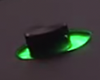
The pedals are going to connect to the jacks. I did want to mount them onto the pcb, so they are secure. Because they are quite loose on my breadboard. Any slight movement can disconnect them. I understand that you say I need to build my enclosure first, I do really. I just want to get this pcb somewhere close before I make them. I have an idea how it will work in my head. I noticed that the +5V and the ground wasn’t connected on one of the earlier sketches but completely forgot to connected it. My plan was to use a wall wart to power everything. What other way can I power the neo pixels? These are the pedals I am using and also the jack I am using.


↧
Creating Ground Vias
Oh OK, yeah that’s what I’m referring to. So I don’t need to worry when I create my ground fill and Fritzing places those directly under existing traces and components on the PCB?
↧
Creating Ground Vias
If you are seeing them under a trace it is likely on the opposite side on the solid part of the ground fill. So yo do not need to worry about them at all.
↧