You can check the Gerbers to see what is really there, which is something you must do before you send it to fab anyhow. I use the free SW, Gerbv.
↧
Creating Ground Vias
↧
Creating Ground Vias
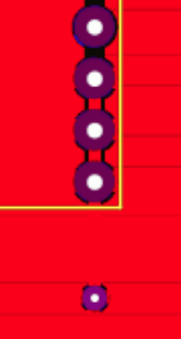
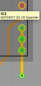
Ok, interesting. I ran ground fill and popped it into the SeeedStudio gerber viewer (this is where I’ll order my boards). Those ground points are gone (great!), but what I’m seeing now is the traces to my ground vias now seem to be just ‘absorbed’ into the ground plane, whereas what I expected was the for just the ground via to be connected to the ground plane, with traces appearing normally just like the rest of the circuit. And it looks like the pins that I’m trying to ground on the components themselves have sort of become their own ground seeds. Here are two images to illustrate what I’m talking about (the red one is from the Seeed gerber viewer). Is this expected/OK?
↧
↧
Schematic to breadboard layout
The issue here is that changes to one thing affect the other, so you want to have something like perhaps a mock up in cardboard of the enclosure that isn’t a huge cost or amount of work that you can change easily and cheaply (enclosures are typically expensive if you make a mistake) along with a cardboard mock up. print a copy of one side of the pcb layout (to get the position of the mounting holes), tape it to a piece of cardboard or a thin sheet of rigid styrofoam and poke the components in to the pads on the paper layout to mount the components. That gives you an easy (and changeable) version of your pcb and verifies that the components will actually fit on the board in real life (both useful things). You will likely have to iterate around this loop (enclosure mechanics, board layout) several times to get a working design. For instance its possible that you will do an enclosure and a pcb layout then discover that there isn’t enough room on the pcb to route the traces, meaning you need to move components which affects the enclosure design. It is much better to get it right with a cheap mock up in cardboard than cut an expensive board on ly to discover it doesn’t work and have to redo it. I’d be inclined to start with the enclosure mock up then see if you can place the components and route the pcb to match that design (if not you need to change the enclosure design).
That was a potentially fatal error. If I hadn’t remembered to look for a source of +5V (because Fritzing will happily let me add VCC tags in schematic without a source of power to drive them) you would have routed the board and it would show routing complete but not actually work, because it didn’t have a connection to +5V anywhere. You should verify every wire on your physical breadboard is also in the Fritzing breadboard view as I expect those two wires are on your physical breadboard (because it works) but not in Fritzing (which is a problem). Note that you need to make this change in all your sketches as well so if you end up using one of the other ones you don’t hit the same error and not catch it before you buy a board.
Have you connected the neo pixels to your breadboard set up and run them? It is possible (but I think unlikely, although I’ve never actually used neo pixels) that they take less current than I expect. I do know from articles from people using them they have ugly power draw issues due to how they work. The issue is the 5V connection from the mega can only supply a limited amount of current (I can’t see a spec for 5V but the 3.3V is limited to 50ma, to be powered from USB the 5V line has to be less than .5 A and I expect the output pin can only supply 50 ma as well). I expect the neopixels will take a lot more current than that (possibly several amps) but you may have few enough of them that they won’t need that much. From the 2 1000uf capacitors, someone expected the neo pixels to draw a large amount of current I think (whether they are correct or not is another matter  .)You would need to check the specs for the neo pixels you use to see what their maximum current draw is (and I would size the power supply to the maximum current draw!). If the mega can’t supply the 5V to the neo pixels (which I think is likely) then you need to be able to supply the 5V for the neo pixels some other way. A 12V multi amp (sized to match the neo pixel draw) wall wart will supply the 7 to 12V the mega needs and one of the ebay buck power modules (there are fritzing parts for several in parts submit, but I don’t think in core) will reduce the 12V from the wall wart down to the regulated 5V the neo pixels need. From your point of view that means you probably need to add a coax power jack to connect to the wall wart in Fritzing, which is the source of 12V. A 1n4004 diode and a 100UF capacitor then connect 12V to the Vin pin on the mega (this should be able to power the mega from what I see in the mega reference schematic and the diode and cap isolate the mega from 12V voltage fluctuations caused by the neo pixels). This forum thread:
has pointers to 2 such converters (limited to 2 Amp output I think) that have fritzing parts and are available on ebay and others. You would need to verify that 2A is enough current to run the neo pixels first (and find a higher current model if not). Now the 12V input from the coax jack goes to the input side of the buck module, and the output side (which you need to adjust to output 5V before connecting the neo pixels!) provide the +5V to the neo pixels (with probably just 1 1000uf capacitor). Assuming you can use one of these converters a 12V 1A wall wart should be fine (cheap and common) as that would provide about 3A at 5V via the buck module. You should modify both your physical breadboard and the Fritzing sketch to add these things and then test the physical breadboard to make sure everything still works correctly. Then you should be ready to do the component layout in pcb (as there are now a few more parts) and see how you can make the enclosure once you have everything you will finally need connected up.
Peter
↧
Creating Ground Vias
Once you have set a ground seed on any net then everything in that net is part of the ground. If you do not want your actual ground pins to be connected then you would use copper fill. This is what is to be expected and what is wanted since you told it that you wanted that network to be part of the ground plane.
↧
Creating Ground Vias
Ok, thanks for all your help!
↧
↧
Creating Ground Vias
Ok, so likewise if I choose copper fill and inspect the nets, my ground vias are clearly connected to the copper fill. But what is the fill grounded to? My hunch was that one of the ground pins on my MCU would have been connected to the copper fill, but that appears not to be the case. Maybe I’m overthinking all this, I’m just trying to make sure the board is correct before sending it out.
↧
Creating Ground Vias
(post withdrawn by author, will be automatically deleted in 24 hours unless flagged)
↧
How to make PCB Arduino Uno Shape
Awesome!
Is there anyway to get the ICSP pins on there?
Thank you both!
↧
Does an Arduino Uno Mega Shield SD Card ICSP SPI Exists Already?
Hey welcome back! Hope your ankle is better.
So my schematic is right…?
Can you take a look at the link I posted above and confirm this is the correct part? If it is, there must be something that went wrong with my surface mount soldering.
↧
↧
How to make PCB Arduino Uno Shape
Nothing automatic. You could search for “generic” in the parts bin and then use a generic header. In the inspector you can change it to double row.
↧
Creating Ground Vias
As old_grey said copper fill is not attached to anything. Only ground fill connects to the ground fill seed. If you want copper fill but connected you will have to connect it yourself after running copper fill. You can either connect it to one of the red dots like old_grey said or you can drop a via somewhere over the copper fill and connect a trace to it.
↧
How to make PCB Arduino Uno Shape
You can use the ruler to position the std header, like sub said, other wise you have to get the UNO svg and delete what you don’t want and import it into a new part.
↧
Creating Ground Vias
Thanks, it all makes sense now. So it seems that if I’m choosing to go the Ground Fill way, I don’t even need the additional vias, I can just set ground fill seeds on each component. Is that ideal?
↧
↧
Creating Ground Vias
Since all of your grounds should be connected into a single net by traces you should only need to set the seed on a single point and everything that is connected to that net will be part of the ground fill.
The need for extra vias is on a board to board basis. For example you may have an area of fill that does not actuall connect to the ground net because it is surrounded by other nets. In that case you can add a via to connect it to the ground fill on the other side. If the area is small enough you can even delete the small section of ground fill. But this need for them to be all connected depends on what type of circuit you have and how much noise there may be. In most cases unless you are designing high speed communications circuits you do not need to worry to much.
The other reason for adding vias is to move heat from one side of the board to the other. So if you have a voltage regulator or FETs that are dissipating a lot of heat you can add lots of vias to move the heat to the other side of the board. There are many more things that you would want to keep cool those two are just some common examples. If you unsure if a component needs extra cooling check the datasheet for the thermal recommendations.
↧
Does an Arduino Uno Mega Shield SD Card ICSP SPI Exists Already?
The different pin numbers on the socket confused me. miso (DO on the socket) shouldn’t be level translated and is in the wrong direction. DO is the data back to the micro and will make this not work. VCC needs to be 3.3V and the IC a 74ahc125 and pin 12 of the 74ahc125 needs to be grounded (as it is unused and cmos doesn’t like floating input pins). This site has a wiring diagram for an SD interface. Here the 74ahc125 is the level shifter in the schematic.
edit: (forgot to actually add the url …)
https://openlabpro.com/guide/interfacing-microcontrollers-with-sd-card/
edit2: the shield pins likely all want to be grounded as well. It may work ok without that but grounded is better.
Peter
↧
APA-102-2020 - the ultimate smd addressable led
hello, be careful the number after 2020, 8192 of this part
means “grayscale” , there are integrated system that map your (1-255) grayscale to (1-8192)
with integrated gamma correction
the problem is, it uses a pwm much-slower to create the 8192 gradient, that there are gaps and flickers like ws2812, and thus this type of package is not suitable of POV devices
find some like apa102-2020-256
↧
Schematic to breadboard layout
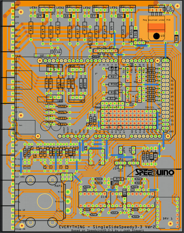
Hello, thank you for your reply. And sorry for replying late, I have had a busy week. Anyway I have been working away on this project. I’ve been working on the casing so hopefully that might be made really soon. I’ve also been trying to work on the PCB. I have been moving a few things around and also changing pins 13 and 46. But I am still having issues, I can get the PCB to fully route when using auto route but obviously it makes a mess with the traces. But the main problem is traces and parts getting in the way of each other. Could anyone help me out? I’m really been struggling. I’ve also been looking at other software too. Chewie original circuit.fzz (129.3 KB)
↧
↧
Schematic to breadboard layout
There is no such thing as a good auto router, even with $9K software, so everyone should be manually routing.
This took days, but it was worth it.
↧
Schematic to breadboard layout
I know auto routing is a bad idea, I have tried moving the pins about for the pcb layout. I have moved them on BB view then corrected the schematic. The schematic isn’t the tidiest but I didn’t have much time. Would someone take a look please. Not sure if I have broken the schematic view thanksChewie original circuit edit.fzz (136.2 KB)
↧
Schematic to breadboard layout
I can’t fix it because i don’t know about electronics, all i know is when i see something strange in FZ.
I see a ratsnest in BB on the Mega. I think you must have forced a connection in SCH and it thinks you now need that connection, or one of the wires in BB isn’t actually connected so FZ is putting one in.
The junctions aren’t text book, so it’s hard to know what you intended. If you look at the R27 there is a big junction on pin i but a small ones on the wires below. Big junctions signify a double or more connection, where as a small one is just a bend in the trace, and because there is on big junctions on the traces below you are never sure what is actually connected. I think I mentioned it before, but you run a trace from a part pin to a bendpoint, or you hold ALT and click on a bendpoint and make a trace to the part pin. Then grab the big junction and move it around and check all the traces stay connected and move with it - 4 junctions are a bit weird and don’t all move -.
Other rules is that you always have a black trace between parts, ie no part pin to part pin, and no part pins sitting on traces, eg R28. This like that can lead to thinking you have a connection when you don’t.
Other than those fine points it looks pretty neat.
If you want to switch to other EDAs they don’t have a BB view, which is one less headache to worry about, and they force you to do the whole SCH first and export it into PCB view, which has less chance of errors, if the SCH is correct, because the views aren’t connected.
↧