I would agree with what Peter said about the corners and running the DRC. Peters version may have solved the DRC issues by reducing the traces that go between the pins to 8mil but I would go a step further and make the board a little larger (1.5mm) so you have room run those traces around the outside and avoid going between pins unless absolutely needed.
Here is what I came up with quickly. I turned off the snap to grid feature as I do not like it. I moved 1 resistor to make routing better. I added 1.5mm to one direction to make room to go around the header pins rather than between them.
Also I would not use Aisler to make the boards. It does not seem to help Fritzings development seeing as how even those of us involved can not get a hold of anyone in charge and development has all but stopped so I see no reason to pay 20 times as much for PCBs to them if that extra money is not going into Fritzing. I get my boards all made at Elecrow and it only cost $4.90 for 10 high quality boards with your choice of thickness and color etc. Here is my affiliate link Elecrow If yiou use my link I will get a few points I can use on my next PCB order. You will find the same prices from other places like Seeedstudio and Dirty PCBs
Also I would not use Aisler to make the boards. It does not seem to help Fritzings development seeing as how even those of us involved can not get a hold of anyone in charge and development has all but stopped
Sounds fair. I’ve read about a somewhat troubled development history of Fritzing and that’s really sad for a great piece of software like Fritzing.
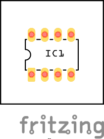
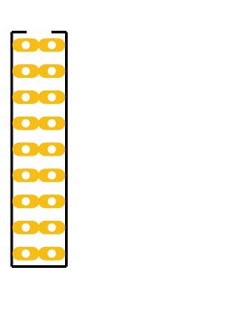
I started from a different footprint that I had modified (incorrectly it turns out ) for someone else a while back. I’ve been testing and fixing things I found wrong until I think these are good enough for now. For others reading this, I want to change the parts factory to use this as the standard IC (and possibly header too) footprints so if you see issues, speak up. In any case here are the three footprints you wanted. As usual the forum doesn’t like the svg, so they are posted as fzp files that you need to download then rename to .svg.
I am new to this software. After I download and unzip the file. I double click Fritzing.exe to start the programme. It always show “Not responding”. I deleted the file and downloaded twice, the problem still exists.
Did you wait the 10 min for it to download the part update when you installed it. It shows no progress bar when it does so people mistakenly close the program down before it completes, thereby damaging the install.
Hello Peter.
Thank you again for your efforts. I’m not sure if I should like the squared pin 1, but hey, your graphics - your rules
May I kindly ask you some questions as I would like to learn more about part design?
a) How do you achieve the grid alignment in Fritzing?
I see that the top/left pin is at 50/50 (I assume 51.041668 is just some mismatch) but what measure keeps it perfect in the 100/100 mil grid of the PCB view? Based on the numbers I would expect, that the part aligns in the middle of the box - not at the corner. I don’t find any hint in the XML to get that offset from 50 to 100. How do you do that?
b) Is there any reason why you draw the parts in “landscape” not in “portrait” dimensions? Portrait mode will give pin 1 the position top left.
c) hole measurements in general are miracle to me
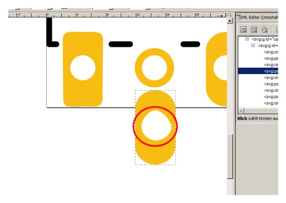
the holes are circles defined with r=22.5 with stroke 10. That should be 22.5*2=45mil Minus 5 for half the stroke (?) leaves 40mil = 1,016 mm as drilling hole? Is that correct ? The fab will produce a 1mm hole?
The reason I want to clarify: I want to make a part with two rows in line (100mil) and the oblong pads are to large for a 100mil grid. Even the round standard header holes are to large for routing standard wires between them. So what would be the best hole definition for a 1mm header? To be precise: the header measures 0.64mm/0.025mil. Should I just take the r=22.5 with 10mm stroke - but that’s against the “fritzing graphic standards” as they suggest 20mils at least. source: http://fritzing.org/fritzings-graphic-standards/
d) i found that the hole in the pad is not really a circle, it’s more like a Easter egg ;-). I know it’s already in the very first sparkfun part, but just want to warn you if you want to do more parts with that pins (and I see even my generator generates Easter eggs).
If you don’t like the square pin, in a text editor (or the Inkscape XML editor) just copy the d parameter of the path for pin 1 in to the d parmeter of the path for pin 0 and change the first parameter after the m to 1 less (from 151 to 51 if I recall correctly) and you will have all the same pads. I usually like pin 1 to be different so chip alignment is obvious. That is one of the nice things about Fritzing, if you don’t like a part you have the source and can change it suit you better.
Sure, that’s how I learned parts design (as there isn’t much good documentation around) and pretty much the only way so far to learn the various corner cases.
Usually with difficulty and often by trial and error . This is one of Fritzing’s oddnesses and I haven’t yet dug in to the source to see what really happens. In theory alignment is thought to start at pin 0, but tests tell me it is more complex that that. There seems to be some kind of voting operation (or possibly a bug) that means if you take a 4 pin chip in .1 in alignment and move pin 0 (which I would expect to change the other 3 pins alignment relative to other pads on the board which is the usual case I’m dealing with), only pin 0 changes alignment. At some point of moving the other pins does change alignment relative to the rest of the board, but I haven’t figured out how yet. The other part to this (and I think what you are actually asking here) is that Inkscape aligns to the edge of the graphic where fritzing aligns on the center of the graphic. Meaning that if you need to horizontally align graphics with different widths you need to calculate the position of the center of the graphic and make sure that is the distance that Fritzing is expecting. The usual case where pads are all identical width is easy, just make the start of each graphic the offset distance you desire, except that in Fritzing there will be a 1/2 width offset to where the part starts compared to what Inkscape displays, but that usually won’t matter as long as the drawing is internally consistent. You just need to remember that the coordinate systems are based differently.
Not a good one . I usually just go with whatever the drawing I started from uses as doing rotations (at least in Inkscape) usually causes transform/ translates. Common sense (but no actual measured data yet) tells me transform/ translates are undesirable, as at render time they incur a matrix multiplication which is a performance issue. I think it is worthwhile to remove the translates at part creation time (where it happens once) rather than at render time where it happens at every render (which Fritzing does a lot!).
It is pretty easy once someone explains it ( @steelgoose in this case) but it differs between editors. Luckily we both use Inkscape so there the equation is:
So for one of the 0.035 in holes in the pad with dimensions in inches, click on the circle in a pad and the length/width in the tool bar will be 0.055, from XML editor stroke-width is 10 thus
0.035 = 0.055 - (2 * 0.01)
It looks like you need to add the stroke width to the 2 * radius value from xml editor to come out right i.e (22.5 * 2) + 10 to get
to the correct 55 . That said, there is a twist because I think that Inkscape uses the python math library and the “almost equal” floating point compares which return equal from a percentage
range of values to avoid roundoff problems, so if you set the sizes with dimensions in inches and make all the circles the same size and spaced .1 in, then switch to px (which is finer resolution) you will discover the values vary by a bit. This translates in to a slight (and mostly insignifigant) variation in the gerber output coords. To get the coords exact as in these footprints I change the tool bar to px (the highest resolution Inkscape has) and make sure the intervals in px are all the same. The easier way to do this would be in a script, such as the part check python script, that adjusts the connectors (if requested) to be evenly spaced, but I haven’t done that yet.
My footprint actually violates the standard too , it is the only way to get the pads to work, so yes if the 10mil stroke width works (and most importantly creates enough copper to allow the solder joint to support the connector on the board) then it should be just fine. To a large extent we are pushing Fritzing past where its original intent was, and sometimes the standard gets in the way. I would adjust the hole in the path that defines the oblong pad to move the hole that uncovers the hole in the circle closer to the edge of path so the hole moves toward the edge of the oblong (and the opposite direction on the facing pad) so you have the same pad area but with the holes better aligned. If this doesn’t make sense I can modify an svg to do what I mean and post it (a picture is worth 1000 words ). I’m too lazy to generate a png file from this but here is the xml to replace the d field in a path to do what I mean:
m 150.5,317 c 15.18783,0 27.5,11.6406 27.5,26 v 52 c 0,14.3594 -12.31217,26 -27.5,26 v 0 c -15.18783,0 -27.5,-11.6406 -27.5,-26 v -53 c 0.56862,-13.96744 12.71582,-25.01034 27.5,-25 z m -18.7161,39.12924 c 0,8.83656 9.32726,16.85804 18.7161,16.85804 9.38884,0 17.85805,-13.16979 17.85805,-22.00635 0,-8.83656 -6.75311,-16.85804 -16.14195,-16.85804 -9.38884,0 -20.4322,13.16979 -20.4322,22.00635 z
If you replace the d value of a bottom pad on one of the footprints with this it should offset the pad down a bit in the way I intend which should make your header part work as you need (you would need to go the opposite way for the pins on top).
Yes I know. That is what the "I think these are good enough for now. " comment is about. The correct answer (again for performance reasons) is to eliminate the circle overlaying the path and adjust the path so the circle is a circle of the correct radius to generate the correct hole in the gerbers. That way we save the time to render a redundant circle and performance gets better (and the part file size gets slightly smaller, both good things). The difficulty is in the details though. I know that the gerber code can create holes from just a path (because I’ve seen parts that do it) but I don’t know enough about path creation to be able to do that yet and it looked like learning it was going to take too much time at the moment. If you have more questions feel free to ask. Doing this here helps anyone making new parts and more people making parts is good (more people interested in helping develop would be even better!).

 ) for someone else a while back. I’ve been testing and fixing things I found wrong until I think these are good enough for now. For others reading this, I want to change the parts factory to use this as the standard IC (and possibly header too) footprints so if you see issues, speak up. In any case here are the three footprints you wanted. As usual the forum doesn’t like the svg, so they are posted as fzp files that you need to download then rename to .svg.