Quantcast
Channel: fritzing forum - Latest posts
Viewing all 30896 articles
Browse latest View live

Custom Shaped PCB crashing output

$
0
0

You are doing better than I :slight_smile: for me the contour layer is empty:

Fritzing pcb:

Gerbv output has no apparent contour layer (although the file is loaded):

In any case, it looks like you have hit one of the gerber output bugs and need to try and adjust the outline svg to make gerber output happier.

Peter


Custom Shaped PCB crashing output

Using property names in part creation

$
0
0

That works for me. Your previous post said fritzing.org. Nothing there mentioned the wiki, which is on github, not frizting.org.

So I added wiki as a place to do the work. Yes I contributed there before, but it was to add one line that was obviously missing. I did not feel official enough to do much more. If WE are going to be expanding that, the first thing I would like to do is add some more navigation and cross referencing. That is written like a hard copy book. At least like a chapter in a book. With web and links, some table of contents and other links can make locating information a lot easier.

If that is the direction forward, unless there are objections, we could also use a thread (or several) in the repository issues for discussion about organizing, missing content, other references, etc the wiki page content.

@vanepp

Or have an id, then reference that in the schematicview section of the fzp file. Add a labelId attribute to go alongside terminalId. That by itself could be enough to enable editing, and also provide a fine grained method of selecting only specific connectors for label editing.

Whoever is doing the work on the svg better consider what placement is going to look like if the string length changes. Set the appropriate text alignment.

Using property names in part creation

$
0
0

Actually it seems to work fine. The update went in without problems and everything appears to work. Started with this test sketch with the original part:

test-orig-master.fzz (8.6 KB)

Then installed your new repo, regenerated the database and loaded the sketch:

Capture

yes

Capture1

Compressed a bit as you moved schematic back to .1 boundaries, but handled fine (so possibly the problems in update I remember seeing are bad part configuration, not a bug.)

Setting dot size narrow via inspector moves in breadboard, but a reposition fixes everything:

Then I ran through all the combinations in Inspector and checked DRC and appearance, and except for sometimes having to move things everything looks fine. One thing I did notice is when changing matrix size in any view I get a message on the bottom of the screen “No exactly matching part found: fritzing chose the closest match” but the change appears to work correctly. So I’d say this looks fine so far.
As to github, I started from a clone of the parts development repo, in to my fork on github, cloned that locally, created a branch and made and pushed a part. It got merged, but Kjell made a few changes, so I tried to resync my repo with those changes but wasn’t successful. As part of that I did set an upstream value (I currently don’t remember how to display it) and did fetches of various kinds without success. I’ll try your command set and see if I can get the three ins sync and do another pull request and see what happens.

Peter

Part update pcb view mess, possible corruption in sketch

$
0
0

Testing the update process for a part being obsoleted worked with a simplified test sketch, but a slightly more realistic sketch lost connections and traces in the pcb. There was a bit of minor cleanup needed on the breadboard view, that amounted to moving breadboard and updated part slightly to get them to reconnect. Schematic view updated fine.

@vanepp I figured this belonged in its own topic. Probably nothing to do with property names :slight_smile:

The sample drawing and update were done using Fritzing 0.9.4b commit c595162a1d0 on a full up to date Fedora 31 workstation.

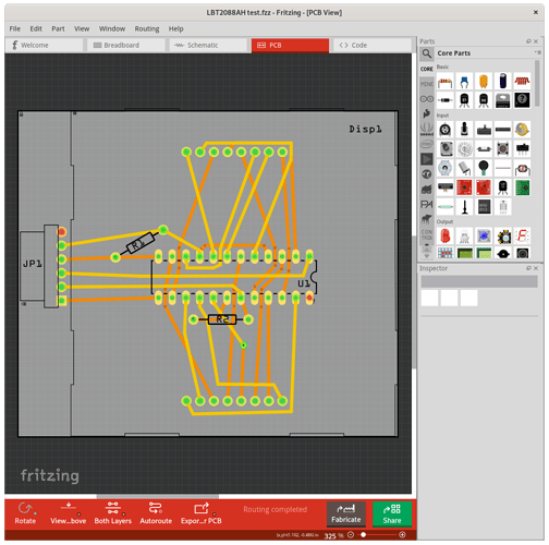
Here is what the pcb view looks like before the led matrix part is obsoleted. Don’t try to make sense of that as normal pcb. This was for an experiment to mount the controller chip directly on the back of the led matrix, and use direct point to point wirewraping instead of pcp traces. This just provides a visual tool for planning the wirewrap connections. Though I was pleased to find I could layout the pcb with only a single via.

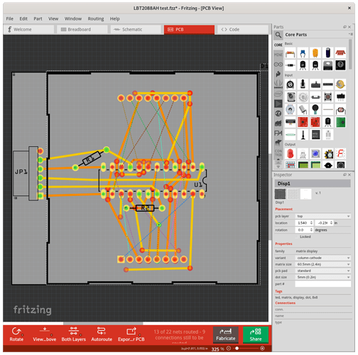
Here is what it looks like after the part was obsoleted, the sketch reloaded, and the part updated. All connections are now ratsnest lines, and many of the traces (especially top) are missing. Others are missing from some of the bend points.

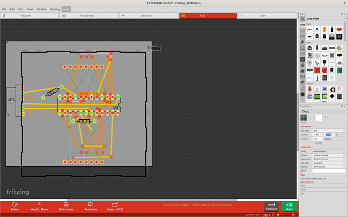
Here is what it looks like with the led matrix part moved left 0.1 inch and down 0.2 inches, showing that the traces that remain are not actually connected to the part.

Attached is the drawing, from before the update was done. To replicate the steps, you will need to use the 8x8_led_matrix branch of my fritzing-parts repository. That is where both the new parts, and the obsolete LBT2088ah part exist.

LBT2088AH test.fzz (28.0 KB)

git clone https://github.com/mMerlin/fritzing-parts.git --branch 8x8_led_matrix

Anyone have ideas on what would cause that sort of breakage, when both the new and obsoleted part have been shown to work in a simpler drawing?

test-orig-master.fzz (8.7 KB)

Extra information. Many of the open ended circuit traces only partly exist. Trying to move the end point, or add a bend point causes them to vanish. The board design was done in the schematic view, except for JP1. That was connected after most of the pcb board routing was finished, and it became obvious which connections would most easily reach which pin. There isn’t really a molex connector there. Just a bundle of wires going off board.

New Part THT & SMD problem

$
0
0

Yes, AI saves the xml like that, what unit I currently using or something… But never had a problem with that…

Anyway I missed the main problem with SMD…
They all working smoothly if I use the parts on TOP layer of the PCB.
But, whenever I move it on the bottom layer, the SMD pads still connecting with TOP layer trace…!!!

Not only my parts, even the core parts…
Here, a screenshot with same part (sparkfun usb connector) on different layer connected with TOP traces…
Maybe it’s a creation Failure…!!!

Also, obviously problem on THT+SMD part…


If a good part, like SMD IC, can work perfectly with only copper1 layer, It should be work as well as on combine parts (THT+SMD)…

I think, there must be a missing rule in the software, that it cannot change layer when “copper1” & “copper0” both are active…

Or, I’ve to test, as you previously said to keep the copper group separate instead of making them parent/child…

Part update pcb view mess, possible corruption in sketch

$
0
0

Fixed. There are a couple of problems. Started from the original sketch and said no to upgrade. Align to grid is off in breadboard and pcb. Enabled it in both of them. Tried changing the breadboards from tiny to half, and ran in to a bug where the breadboards don’t swap correctly (likely because of different pin numbering). Marked that on my bug list, and went for plan B: moved the current breadboards down and up a bit to make the connections more visible. In pcb set align to grid on, unlocked and moved all (or most) of the parts so they align to the grid then locked them again. That breaks DRC, because the between pad runs are too close with the 0.05in grid size, so reduce that to 0.01in and moved the through pad traces til DRC passes. Save that here:

LBT2088AH-test-new-breadboard.fzz (28.4 KB)

Now exited Fritzing then restarted and reloaded the above .fzz file and said yes to replace. Now breadboard is correct without change (likely due to align to grid), as is schematic after straightening the lines for the reduced pin alignment. Pcb is more messed up. So View disable rats nest lines so as to not create connections from the rats nest lines. Then move the end of the unconnected wires back and forward on to the associated pad to remake the connection and all reconnects correctly and DRC passes.

LBT2088AH-test-new-breadboard-fixed.fzz (28.2 KB)

come to think of it rats nest in pcb is probably still off in this …

Peter

New Part THT & SMD problem

$
0
0

Before I got distracted in to the display obsolete part issue that I just fixed, I had though of this and was about to try your part on the bottom of a board. You likely need completely separate copper1 and copper0 groups (not copper1 as a subgroup of copper0 which I think is the current configuration.) The SMD pads need to be only in copper1 and the through hole pads need to be in both. Then I think swap top to bottom may work correctly because copper1 will be as Fritzing expects it. Luckily for me you found the problem first :slight_smile: so I don’t have to poke at it.

Peter


Can´t find chip ESP32-WROOM and ESP32-WROVER

$
0
0

Hi
i´m looking for a new popular microcontroller from Espressif that i have made som really fancy stuff with. I can´t fint this in the libary.

Anyone that can support making the chip ESP32-WROOM and ESP32-WROVER ?

product information of ESP Modules

Thanks

Part update pcb view mess, possible corruption in sketch

$
0
0

I had both forgotten I had turned that off, and did not know it would cause problems when updating the part. I turned it off on the breadboard view, so I could get the led matrix pins to align to the 2 separate breadboards. Turning the alignment grid size down as you did is another option. On the pcb, as you discovered, the space for the traces is tight, so again I turned of the grid alignment to gain (zoomed in) positioning freedom. I’ll have to adjust my process to use small grid spacing instead.

Also, that needs to go into usage documentation. If minor alignment / positioning differences are going to break part updating. Both as a strong recommendation to keep aligned to grid, and as a step to try if updating parts breaks things.

It is very hard to setup a breadboard numbering sequence that does not break when the size changes. Because the total number of pins changes, and the rule is that they are supposed to stay sequential.

If we could start at zero for the groups of five, and increment enough to handle the largest breadboard, then skip ahead to a convenient number (say 1000), and start a new sequence for the side connections, jumping by 100 for each group, then they should all be able to stay lined up. Otherwise you need a breadboard to breadboard pin mapping, similar to what is used for updating obsoleted parts.

Normally I would say you need that mapping for every breadboard, to every other breadboard. But, mapping each breadboard to that theoretical breadboard, matching the numbering pattern suggested above with gaps, would allow a 2 step mapping to work. So, define a fake breadboard with 200 groups of 5, and 8 groups of 100 (to handle the breadboards with the split in the middle of the side groups), with numbering from 0 to 1799, and map the connections of every real breadboard to that. That mapping could be shortcut drastically, if there was a way to specify the start and length of a sequential sequence. For the half+ breadboard, map
0 to 0, and continue for 150 entries, map 150 to 500, and continue for 150 entries, map 300 to 1000 and continue for 25 entries, map 325 to 1100 and continue for 25 entries, map 350 to 1200 and continue for 25 entries, map 375 to 1300 and continue for 25 entries. That would be a lot shorter than doing 400 pin mapping entries. Because the pattern is consistent that could even be reduced to just [0, 150, 300, -1, 325, -1, 350, -1, 375, -1], specifying the starting connection number for each connected group (of groups), with “-1” because the side groups are not split. With the right code, [150, 25, -1] is enough.

To improve that, might need an offset value, for how far the side groups are offset from the 0 row. Though simple centering should be very close (and a pain when that does not land on the 0.1 inch grid).

That can be used to match pins of a breadboard to any larger breadboard (up to 100 rows long). The other direction, there will be some truncation. Bonus if you (user) can specify an offset, so the middle of the bigger breadboard maps to the smaller one, instead of starting from the end.

Same kind of issues with strip boards, but I don’t think a general solution is possible for them. There are too many different connection patterns to create a general mapping.

Doit esp32 devkit v1 30-pin

Doit esp32 devkit v1 30-pin

Doit esp32 devkit v1 30-pin

$
0
0

ok thx, i think i have a solution for every of all my esp32 boards now…

5 pin XLR not found

$
0
0

Hi all
New here at the forum, using fritzing for some while.
Now I’ was looking in to the new part editor but i can’t figure it out.
I’m looking for an XLR 5 pin pcb mount connector (neutrik NC5FAV https://www.neutrik.com/media/8324/download/nc5fav-3.pdf?v=1)

is there anyone who can help me make this piece

kind regards

martin

Can´t find chip ESP32-WROOM and ESP32-WROVER

$
0
0

A google search for “fritzing part esp32-wroom” turns up several hits and a forum search for “esp” turns up several. For the Wroom likely this one (although I didn’t check the number of pins or layout):

The WROVER appears to come in a variety of sizes, so you would need to specify which exact one you want since we would need to modify the part above to match very likely (if the form factor is different.)

Peter


Part update pcb view mess, possible corruption in sketch

$
0
0

I didn’t know that it would help, just that it couldn’t hurt :slight_smile: . Some of the breadboards are slightly misaligned (on my list of things to fix) by not being exactly on .1 boundaries. It may be that the wire reconnect is depending on the snap to grid function (or may not :slight_smile: ) which is why I tried it. I moved the breadboards because I seemed to be having trouble getting both sides to sync at once (one side or the other would but not both) indicating an alignment problem. Moving them didn’t snap to a grid leading me to check that.

No disagreement there, although first we need to find someone willing to write and capable of writing usage documentation :slight_smile: and as usual someone hasn’t appeared yet.

They are set up in groups now (there are potentially problems with some of the odd ones I have made for people over the years, there are some with 6 pins per row for instance.) The issue was the wires already connected to the breadboard when I resized it, so perhaps the answer will be “don’t have wires on the breadboard when you resize it” because sometimes (larger breadboard to smaller for instance) that just can’t work. I think with some thought the smaller to larger could work, something to consider when I get around to the clean up core parts project (breadboard pin alignment and normalization because most of the setups are a bit different) are on the list.

Peter

Using property names in part creation

$
0
0

The referenceFile attribute seems only to be used by the parts editor.
I read it as “as long as the part does not have its own svg, use that of the referenceFile”.
I don’t think we need to warn it the referenceFile does not exist.

 ...
 2880:  QString PEMainWindow::getSvgReferenceFile(const QString & filename) {
 2881:  	QFileInfo info(filename);
 2882: 	QString referenceFile = info.fileName();
 2883  
 2884  	QFile file(filename);
 2885: 	if (!file.open(QFile::ReadOnly)) return referenceFile;
 2886  
 2887  	QString svg = file.readAll();
 2888: 	if (!svg.contains(ReferenceFileString)) return referenceFile;
 2889  
 2890  	QXmlStreamReader xml(svg.toUtf8());
 ...

5 pin XLR not found

$
0
0

This should do the job. Note you need to print out the pcb footprint and compare it to a real part before ordering boards as it was done from the datasheet without a part. Also if you want the mounting holes drilled you need to drag a hole (from core parts pcb) over the mounting holes in silkscreen and set the diameter to 3.2mm. Also I assumed the 6th pin is the shield, as it shows on the pcb layout but is otherwise undocumented in the data sheet.

XLR 5-pin-pcb-mount.fzpz (38.3 KB)

Peter

Fritzing too small for hires display (3200x1800)

$
0
0

Yes, it’s a DELL laptop with a crazy resolution.
It had issues even with Photoshop though they did fix it (their menus were like 3 mm in height).
Have to say that i have not used Fritzing on that PC for a long time (I do still have it)

Fritzing too small for hires display (3200x1800)

$
0
0

one note: there start to be a lot more “4K” laptops out there now
so expect 3840 x 2160 pixels to become more prevalent in coming years.

Viewing all 30896 articles
Browse latest View live