I think it used to be there, and probably will be again. At present however the web site is fragile. There is no staging environment, it has had no (or at least very little) maintenance for 4 years and changes have to be done on the live web page. I see it has been upgraded to use https recently (it used to be http) and likely the passwords all reset (I had to reset mine anyway!) so work is being done in the background as time and funding permit. Doing more is what trying to improve the donation rate from the current less that .1% of downloaders is about. The code is too complex to expect volunteer help, judging from the lack of any help in the last 3 or 4 years, so funding professional developers looks to be the only way forward. Hopefully the email alerts for replies like this one will start working again too. After I hit the reset password button, I realized if replies from Fritzing were being classified as spam and being discarded I was in trouble, but luckily the reset email did indeed come through, indicating the problem with no email alert to replies is with the forum not spam discard and hopefully will get fixed.
Hopefully you printed out the new pcb footprint and compared it to a real part, because if it is wrong (which it may be) the board will be too …
You are most welcome. Keeping people interested in using Fritzing is the only way it is going to survive going forward.
If, like me, you have landed on the download page and have paid a donation, but are not seeing any download options, try this:
Create an account on Fritzing.org and log into it. Then you go back to the download page and you will have an option to download “I have already paid”.
Select that and click Download to get the list of links to actually download the package.
As well if you are logged in on the Firtzing site already you will (or at least I do) get a “there is a problem with your account” error when trying to log in to the forums. I needed to log out on the Fritzing site in order to successfully log in to the forums.
Well, personally I don’t like the fact that the download page is currently setup the way it is… Lots of people help with this project. So access needs to be a bit more open. This is GPL code. So I’m not sure the download page is GPL friendly. I don’t like any of this
Click on the link above to get your software…
Go to github and download the release, that is how you should be getting this software to begin with. Learn how to use GITHUB ie;
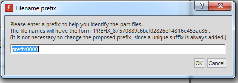
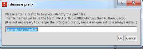
Here we are going to look at the correct layout of the various svg files, because I saw a post from someone that had at least tried to make their own new part before asking for help, that couldn’t figure out the copper layers in pcb. Someone else requested a howto using the parts editor (I think perhaps thinking that parts editor would avoid the use of an svg editor which is unfortunately not correct.) So here I am going to start with a part created from the Parts editor (rather than my usual practice of creating one from scratch) as that is the recommended way to do this. I’ll then at least try and finish the part with the parts editor (although I am usually not successful at that.) The new Parts editor was not completed when development stopped, as a result there are a number of things it won’t do, and probably a number of bugs and I tend to not use it, but it does have the advantage of producing the necessary svgs correctly (if messily) formatted for a new part. It also allows you to set the metadata easily via the metadata tab, so I sometimes do that. To kill 2 birds with one stone, someone recently requested a part for a osoyoo Lora Module, so I am going to make such a part starting from the new Parts editor. The starting point is a google search for "osoyoo lora module: to find a data sheet which led to this web page:
which looks to have the needed data: size of the module, and a mechanical drawing of the connectors (quite unusual for these modules!). It isn’t clear that the 3 connections on the right (which are undocumented) are needed, but I will include them anyway in case they are. There are images of a fritzing part for this module (but no actual .fzpz file I can find) which only have the 7 left side connectors populated. To find a suitable part to clone I started Fritzing and entered “wireless” in the parts search bar and hit enter. That brings up the various wireless modules (and a few oddballs.) Note parts editor will not create parts. You must start from an existing part that has svgs with the appropriate number of pins defined, then edit those svgs with an svg editor to change the svg to reflect the part you want. After that is done the parts editor will configure the fzp file from a graphical interface, but does not edit svg files (it will modify the text of an existing svg file but that is all.) Turns out one of the oddballs: Blackberry Trackballer Breakout is the closest to what I want: 11 connections with pcb as .1in header connectors, so start from that. Select it in the search parts bin and right click on it. Select Edit Part (new Parts Editor) which brings up the new parts editor with the part loaded. Select the meta data tab from the top left:
At this point you can close the new parts editor (saying don’t save to the prompts til it closes.) At this point you have all the required files for the part in the fzpz file in the mine parts bin. Now I am going to proceed to edit all the files (if you want to use parts editor, you only need to edit the svg files below, the fzp file can be modified by parts editor.) First you need to export then unzip the part as a .fzpz file. So right click on the new part in the mine parts bin and select Export Part and save it in an appropriate directory. You can now close Fritzing again answering don’t save to all the prompts. Now change to the directory where you saved the fzpz file and unzip it. That will give you the following 5 files:
We are currently interested in the four .svg files (actually the icon file isn’t interesting and will be replaced by the breadboard svg file later.) Lets start with the breadboard svg by opening it in Inkscape which gives this:
Several things of note here, the svg is scaled wrong (0.75 rather than 10.41667), it has a correct layerId of “breadboard” as the top group (it could also have a group such as g25 below which is a group called “breadboard” and still be valid, but it must have a group with the id “breadboard” with the breadboard drawing elements below it to be correct.) It also typically of Parts editor svgs, has many subgroups. They don’t affect anything (except possibly performance in a probably small way) and can be useful to group sections of the svg, however I prefer to remove all groups except the layerId group (“breadboard” in this case) and because we want to rescale this document we first need to remove all the groups (because rescaling reacts poorly to groups.) So select group breadboard like this:
then either click Object->ungroup multiple times, or as I prefer use the keyboard shortcut cntrl-shift-g multiple times to ungroup the entire document. If groups are present Inkscape will use transforms when you move elements and transforms are undesirable (because they imply an expensive to performance matrix multiplication to render.) Doing that results in this:
which turns up another problem: the 11 connectors do not start at 0 as they should, but rather at 10. So we need to renumber the connectors as well as rescale the document to start our new part. Now refer to the rescale howto here:
to rescale the svg to 10.41667 then delete everything except the connectors (because the connectors are all that we want out of the original svg) to give this (the path6 that makes the rectangle and the holes should be deleted too, but I left it in here to show everything else that has been removed because without the path the white lines will still exist but be invisible against the drawing window and they need to be removed too!):
Now create a rectangle to be the board of the lora module, and set its height and width according the module size in the data sheet (i.e. 21mm wide by 36mm high, then move it to the top so the connectors show on the rectangle and set the fill to green to match the board. Now we need to position the rectangle according to the mechanical drawing. To that end I copied a line from the schematic svg in to the breadboard svg via copy/paste, then set the new line (via xml editor and the toolbar to be as wide as the connectors, black, and with a stroke width of 1 (1/1000 of an inch.) like this:
Now duplicate the line, and rotate the duplicate 90 degrees and move both lines so they match the center of the first pad as the measurements in the mechanical drawing are to the center of the connectors like this:
Now move the x and y position of the green rectangle until the distance from the center of the connector matches the offset from the mechanical drawing, in this case 1.5mm from the bottom of the rectangle to the horizontal line through the connector and 2.88m from the left edge of the rectanlge to the vertical line through the connector. To make calculations easier I did an edit select all and resize page to drawing to make all coords positive before doing the calculations, that results in this:
here the horizontal line is at 3.762mm in y, the bottom of the rectangle wants to be 1.5mm lower than that or 2.262mm so set that as the rectangle’s y coord. The vertical line is at 3.572mm, so the left edge of the rectangle wants to be 2.88mm less than that or 0.692mm so set its x coord to that. Now we delete the 8th pad (as unused) and move the 3 remaining pads to the top of the rectangle for the unknown connectors. To position them, duplicate the horizintal line and add 31.5mm to its y coord to give the center of the three pads at the top or 35.262mm. Duplicate the vertical line and set its x coord to be 3.46mm from the left edge of the board or 4.152mm. Now center the left most of the top 3 pads on the two new lines, then set the other two .1in further along in x to set the postition of the top three pads. That leaves the sma connector for that antenna to source and place. I happen to have made an SMA connector for someone in the past (it is posted in parts help in the forums if you do not have one) so I did a copy / paste of its breadboard (after removing the connectors which aren’t wanted in this application) and copied it in to the svg. Positioning it is somewhat painful because you have to add up the various offsets to the conncetors to get the distance from the left board edge the start of the SMA connector as 12.942mm. Then we need a rectangle (with no dimensions on the drawing so guess!) of the radio module. Once that is done set small circles at each pin position to mark the text to the pin. Then create the text for the labels on the pins and the text on the module from the photo in the data sheet. I usually do a copy / paste of text that is correctly configured from another braadboard, then modify the text to requirements (and that is what I did in this case.) With that done, remove the construction lines as no longer needed and clean up the connectors. The board to this point looks like this (with the first connector to be cleaned up selected):
Here we see a number of issues: there should be a solder tab instead of green in the center of the connector, the circle was an ellipse (I had corrected this one before this image), and the connectorId is incorrect. So fix all of those problems like this. Solder tab: change the fill of the connector from green to silver. Change the id in xml editor from connector13pin to connector0pin, set rx and ry in xml editor to 28.5 to make it a circle again. Then repeat this for all the rest of the other 6 in use pads (increasing the pin number by 1 each time.) Once all the 7 bottom connectors are done, we need to move on to the top 3 connectors. Since we don’t know what (if anything) they do, we will not assign them pin numbers at this time, just leave them as circle123 with a white center to indicate there is a hole there. Now to finish clean up start with connector0pin and click the move to bottom icon on the tool bar to move it (and the 6 other connectors in sequence) to the bototm of the xml window. Functionally this makes no difference, but it makes finding the connectors easier for humans and is thus a good practice to adopt. Now all that remains is to do an Edit-> select all, Resize page to drawing or selection, to adjust the viewbox to match the finished image. Then with Edit-select all still active either cntrl-g or Object->group on the tool bar to group the entire image, then in xml editor change the id of the group just created to breadboard to set the required breadboard layerId. Now File->save as and select plain svg and save (clicking OK to replace) and breadboard is complete and looks like this:
On to schematic. As usual schematic is the wrong scale and unsuitable for the current part, so as usual I chose to replace it with the properly scaled schematic template file from schematic template howto here:
So copy svg.schematic.simple-schematic-template_1_schematic.svg from the above howto in to the svg.schematic.ossoyoo-lora-module_dfdc540f3e4633ed4bfde16ac4e28d7e_1_schematic.svg file and edit it in Inkscape. Delete the pins on 3 of the sides leaving an svg which looks like this:
then set the dimensions from px to in and enable the page grid (View->Page grid) and duplicate the existing 2 connections and move them down in y til there are 7 pins on the left side of the rectangle. Then move the rectange down til it is .1 in below the last connector and increase its height until it is .1 in above the first connector. Increase the width of the rectangle by .3in to give enough room in the rectangle for the part label. The end result should look like this (after doing and Edit->select all and resize page):
Since in theory parts editor should be able to set terminalIds from a pin, I chose to delete all the terminalIds (the rectangle on the end of the pin) from the svg and will try and add them via tha parts editor later. So click on the line that connects to the RXD label and set its id field to connector2pin from line52 in xml editor. Repeat this (increasing the pin number by 1 for each pin) for the next 4 line. Now click on the text “label” and change its id from label to label1 (to avoid text substitution which we don’t want.) Then set its text to be “Osoyoo” duplicate it, and move the duplicated text down .1in in y and set the text to “LoRa”, repeat this and change the text to “Module”. This should end up looking like this:
Now we are going to clean up a bit and save this. First as in breadboard, select the connectors one at a time starting with connector0pin and move them to the bottom of the xml window so they end up looking like this:
Now Edit->select all and resize page to drawing or selection to reset the viewbox, then group (cntrl-g) and change the id of the group to schematic to end up with the finished svg which should look like this:
then File->save set the type to plain svg and save it (answering yes to replace the existing one) and schematic is done. Now on to PCB, so edit svg.pcb.ossoyoo-lora-module_dfdc540f3e4633ed4bfde16ac4e28d7e_1_pcb.svg in Inkscape where we find the scale is again 0.75 instead of 10.41667 so ungroup the entire svg and rescale it to 10.41667 as we did from breadboard to produce (note I cheated here and ran the pcb svg through the check part script to covert the silkscreen from white to black so the silkscreen lines will show up in Inkscape.):
Of interest here is the x and y origin values are not 0 (and it is possible the lines on silkscreen will be truncated as a result) so first do a Edit->select all and resize page to content to set the origin to 0 0 before rescaling. Now rescale the svg as we did for breadboard. Now delete all the silkscreen items except for the 1 line which will make up the new silkscreen and the last 4 pads as unneeded. Starting with the leftmost pad select its id and change it from connector13pad to connector0pin. Repeat this down the line of pads (increasing the pin number by 1 each time.) Then select connector0pin again and look at xml editor which should look like this:
There are several things wrong here that need to be corrected. The radius is incorrect, both from the rescale and because the original svg was incorrect. For .1in headers as configured here, the hole size should be 0.038in, which at a scale of 10.41667 and with a stroke-width of 20 equates to a radius value of 29. At present the stroke-width in the style command highlighted is 17.00022316 not 20 so we need to replace that with 20 in all the pins. Then we need to change the radius values to 29 for both rx and ry on every pin (this will cause the rx and ry values to replaced by a r 29 which is what the gerber code requires to drill the hole.) This is the corrected svg with all the pads correct:
Now we need to do the silkscreen. In this case (as in most cases) the easy way to do that is to do a copy / paste of the breadboard svg in to pcb like this:
here do an Edit->copy to copy the breadboard completely to the clip board. Then switch back to the pcb svg and do an edit->paste which (if the Inkscape gods are smiling on you) will copy the breadboard image in to pcb, leaving it in a group called breadboard for easy deletion later. The result should look like this:
First, select the breadboard group and move it to the top so that the pcb connectors appear on top of the breadboard image. Now move the breadboard image until the connectors overlap like this:
now using the silkscreen line we saved, outline the rectangle of the breadboard image with silkscreen lines to produce the needed silkscreen outline like this:
now it is necessary to add the needed pcb groups. They are (at a minimum as here) silkscreen, copper1 and copper0 (which is a subgroup of copper1.) Other configurations are valid and more groups are possible, but for a basic part this is the minimum and usual setup. First we select all the connectors and group them twice (once for copper1 and the second time for copper0) then change the group ids to copper1 and copper0 like this:
Now we need to group all the lines in to the silkscreen group (which wants to be above copper1/copper0 to aid in the selection process in Fritting) like this:
We now save this file as plain svg to complete the pcb svg. While this is the minimal correct pcb configuration for a through hole part, many other configurations will work (they are just more confusing to look at.) As noted the parts editor loves groups and will produce large numbers of nested groups at times. Somewhere in the set of groups you should find a silkscreen group, a copper1 group and a copper0 group (hopefully under copper1.) I find it best practice to ungroup such a svg and then regroup it in to this configuration to make the structure clear. At this point we have the 3 svg files (and an fzp file, which I suspect is going to be broken because I changed the pads in the pcb svg to be pins and changed the pin numbers but we will see) and can now go back to the parts editor to make the new part. Note there is no magic easy button to make parts, you have to go through the above process to make the 3 svgs (breadboard, schematic and pcb) needed by parts editor to make a part. As noted parts editor will not produce the svg files, you need to do that using an svg editor. The parts editor will adjust the fzp file for you, (as noted I usually find it easier to edit the fzp file with a text editor, but this time I am going to attempt that with the parts editor and see what happens.) Start Fritzing and load the ossoyoo-lora-module.fzpz part I started from in to Fritzing in the mine parts bin and right click on it and select Edit with bew parts editor. The editor comes up as expected, so now let us try and load the new breadboard svg we created in to parts editor. To do so, click on breadboard view which currently looks like this:
doesn’t look much like the bb svg we last saw above. So exit this, and run that svg through the FritzingCheckPart.py script (which I hadn’t yet done) to remove the px from font-size (one possible cause of this failure) and inline the style commands (not as likely a cause) then try again. Yep, looks like the parts editor doesn’t like px in font-size (Fritzing doesn’t either, that’s why FritizngCheckPart.py removes them) this time the svg looks correct:
Now to try and set the connectors via parts editor. So change to the Connectors tab in Parts editor. First problem, there doesn’t appear to be a way to change the connectorId. It appears to have taken the connectorIds from the fzp file (which in this case is incorrect, starting at connector10 instead of connector0 as it should.) It appears the only solution to this is to manually edit the fzp file to correct the pin numbering. Given that you have to hand edit the fzp file anyway, I don’t see a point in not doing the entire fzp file manually and thus don’t see any advantage to using the Parts editor to make parts. Here is the original fzp file (where connectors start at connector10):
The problem I see is that the above file in conjunction with the 3 svgs created above when run through FritzingCheckPart.py then zipped in to an fzpz file creates a valid part. There doesn’t seem to be any point to editing it with the Parts editor after fixing up the fzp file manually. If someone who uses the parts editor successfully would point out where I am wrong (if I am wrong) it would be appreciated. The bottom line is that the parts editor (at least in its present state) doesn’t reduce the work of making a part very much.
While I don’t like it either, I see the necessity of it if Fritzing is to survive. Only about .1% of the people downloading the code in the past made a donation with the previous download page, and there needs to be a revenue stream to support the web site, download infrastructure, and development. I don’t think the donation violates gpl, it has always been true under gpl that a fee for a service is fine. In this case the fee pays for the infrastructure to build and publish a distribution (which, having built a build environment for development I can testify, takes at least a couple of mandays of time to do!) You are, as you point out, free to download the code from github, and compile it yourself, it isn’t anywhere near easy, but it is possible. My self I would rather make the donation than go through that hassle (although I have to anyway to do development.) In the 3 or more years that I have been involved in Fritzing, I’ve been watching it die. There are far fewer people participating here in the forum than when I started and much expertise and history has been lost (most of the folks that taught me to make parts are no longer participating here, which is a big loss.) In the 3 or more years since the last release before the latest 0.9.4 release (which is mostly a test of the new build environment) there were only a handful of commits to the code base, because development had basically died. History seems to say that Kjell is correct, that for development of Fritzing to proceed, a revenue stream to fund professional developers is needed, because the code base is too complex to depend on volunteers. To me that seems correct (and I have a couple of fixes in the 0.9.4 release, so I have experience trying to modify the code, it is not at all simple and is pretty much undocumented.) We are between a rock and a hard place, but there is a new release, which will keep Fritzing from dying from bit rot (which was starting to happen, the libraries were getting so old they are unsupported on some systems) for another few years, and hopefully development will restart. That is far better than I have managed to do over the last couple of years of trying to restart development, and I for one am happy to see it happen as I don’t want Fritzing to die.
I don’t think inkscape is quirky, I get along with it quite well considering I am a newbie at it. I think the inkscape to Fritzing interaction needs work and I think most of the problems can be solved on the inkscape side of things.
Anyway, here is my ‘beta’ part, please run it thru your parts checker and let me know if there are any problems. Fritzing pdf export of the PCB silk screen and the left side 14 pin connector line up with the board I have. The 4 pin, right side connector (for the sd card) should line up, but i haven’t checked it because I don’t have a header soldered in there yet.
Quirky is possibly an incorrect term (although there are bugs in Inkscape that I occasionally hit too), I think the real problem is ignorance on my part. I think what happens is I type aiming to change text, without having the text field selected. As a result the text is taken as hot key presses which sets some condition (such as changing the result of a copy / paste operation to paste an image of the original instead of the xml that I wanted) and I don’t know what I did and thus not how to change it back (because it gets set in the preferences.xml file and is thus persistent.) Annoying Inkscape certainly is . Not all of the problems are solvable in Inkscape because Fritzing does not fully support CSS and Inkscape does. The two are fundamentally incompatible and Inkscape has no reason to change (nor any interest in doing so.) The part check script started out to do exactly that (it could also be perhaps be done in Fritzing, but when I first did the script, Fritzing development was stopped with no new release planned.) Since I needed to parse the xml to make the changes, I could also flag and correct errors in parts and over the course of a year or more the script as it stands grew. I am slowly working on making the script more robust to add it to the input tool chain for parts submission on github (i.e. your part will need to be able to pass the scripts checks to be included in core parts.) On to your part.
Mostly very good, just a few issues: FritzingCheckPart.py script output (edited for space, as the output is typically long even for a good part):
Modified 1: File
‘svg.breadboard.2.8lcd_05ce3fb27514cf8fb52325ad444b9354_9_breadboard.svg.bak’
At line 225
Removed px from font-size leaving 2.11666656
… (many more)
The script removes the px from the end of the font-size because if it is there (which is required for CSS compliance which is why Inkscape adds them) when the part is edited or loaded as an svg in the parts editor the font size will be set to 0 (or in the example below to a large value.) There is an example in
when the breadboard svg was loaded in to the parts editor. The font size will be set wrong (typically it is set to zero and the text disappears, in this case it appears to have been set large for some reason. In either case you need to remove the px from all the font-sizes in all the svgs. It is done by the script automatically, but can also be done with a text editor by doing a global remove of “px” (you do need to insure you don’t have a “px” that isn’t part of a font-size though!)
Connector8 doesn’t exist when it must to stay in sequence
The pin numbers should start at connector0 and go up in sequence, that isn’t true here. It is only a warning because it only sometimes breaks the hover on a pin to get the pin label function not anything more serious.
Warning 20: File
‘svg.pcb.2.8lcd_05ce3fb27514cf8fb52325ad444b9354_9_pcb.svg.bak’
At line 42
copper1 layer should be at the top, not under group silkscreen
This is slightly misleading in that copper1 is actually under copper0 not silkscreen, but the order should be silkscreen, copper1 with copper0 as a group under copper1 (at present copper1 and copper0 are reversed.) I don’t know of any problem this causes other than Fritzing will prefer to select silkscreen if it is the lowest group (thus a warning rather than an error.)
While this shows as an error (because in schematic it likely is one), in this case it is ignorable, because Fritzing will use the center of the pin as the termination point as was intended. Technically you can and should remove the connectorxterminal elements in breadboard, but it won’t hurt anything. repeats for all the pins on breadboard.
Error 69: File
‘svg.schematic.2.8lcd_05ce3fb27514cf8fb52325ad444b9354_9_schematic.svg.bak’
At line 16
Found a drawing element before a layerId (or no layerId)
This one is the only real error. The schematic svg lacks a layerId (in Inkscape you need to do an “edit->select all” then Object->group and name the group “schematic”). If this part is exported as an svg, at least schematic will not show up in the sketch due to the lack of the layerId.
Error 74: File
‘svg.pcb.2.8lcd_05ce3fb27514cf8fb52325ad444b9354_9_pcb.svg.bak’
At line 133
Connector connector18pin has no radius no hole will be generated
This isn’t actually correct, because there is a circle (the connectorId is attached to the rectangle which overlays the circle) so a hole will be drilled. But from a usability standpoint it is better to have the connectorId on the circle so someone modifying the part can change the hole size easily.
With that done and no major problems, load the part in to Fritzing and test it. This is to catch errors that the script can not (such as a terminalId existing but being in the wrong place). Here is a sketch of a typical test:
Here all connections are connected to .1 header connectors and routed in all three views to make sure the connections go where expected and the terminalIds (mostly in schematic) are in the correct place. That is the reason for the 45 degree offset of the connections in schematic. If the terminalId is wrong or missing (which the script should catch), the wire will connect to the middle of the pin (or the wrong pin completely which the script will not catch). In this case they are all correct. In pcb view all the pins are routed, and then every other trace is moved to the top of the board (except for SMD parts which only have one side) to make sure both layers are working correctly. Then the resulting sketch is exported as a gerber and checked in a gerber viewer for correctness (in this case I used gerbv from the geda project) as there are bugs in the gerber code that sometimes make the gerber output incorrect even though pcb view looks fine. This is also a good place to check the hole sizes of all the pads, as the gerber output has a drill size table for the holes that will be drilled. In this case your hole sizes are too small. For .1in headers the standard hole size is 0.038in, in yuor part the holes are only 0.035 as we see by exporting the test sketch to gerber and then editing the drill.txt file in the gerber output (it is much longer than this, but the drill sizes are at the top):
; NON-PLATED HOLES START AT T1
; THROUGH (PLATED) HOLES START AT T100
M48
INCH
T100C0.038000
T101C0.035118
%
The top number is the .1 headers in the test sketch, the second number are the pads in your part. To correct that you need to change the dimensions of the pad in pcb view. In Inkscape (the other svg editors are different I think) the calculation is this:
Hole diameter = Pad diameter - (2 * stroke-with of the pad)
In your case using connector0pin as an example that is:
diameter = 0.075in (from the w and h fields in the tool bar when it is set to in)
0.50799996 at a scale of 0.26458 which is a problem, because we need the stroke-width in inches for the above calculation. It is possible to convert this value in to inches. Instead I rescaled the pcb svg to the standard 10.41667 scale (where one drawing unit = 1/1000 of an inch) and did the calculation there. Rescaling svgs is explained here:
Doing that points out the problem. The diameter of your pads is slightly too small, they are around 0.075in (when they should be 0.078in) and the stroke width is 20.00025558. If I reset the diameter to 0.078 and the stroke-width to 20, the holes will be the correct 0.038in. However changing the diameter via the tool bar will move the center of the pad slightly (causing misalignment) so the trick to do is to change the w and h parameters to 0.078 in the tool bar and then record the radius from the xml editor window (which will be 29.) Now undo the w and h changes to restore the pad to its original position and instead change the radius from its current value to 29. This changes the diameter relative to the center of the circle leaving its x y position the same which is what we need in this case. As a side issue the radius is currently an ellipse not a circle (because of floating point roundoff during the rescaling) and thus has a rx and ry in xml editor. We want to change both to be 29 which will make it a circle with r=29 again. Then change the stroke-width to 20 and you are done. Alternately you can do the scale mathematically like this to calculate a new radius and stroke-width at the current scale (but I find rescaling easier):
scale 10.41667 / 0.26458 = 39.37058734598231
so work backwards radius 29 / 39.37058734598231 = 0.736590484291045
So in your original svg setting
each circle to radius 0.736590484291045 and stroke-width 0.5079934374421 will have the same effect, a pad with a 20 thou copper width and 0.038 hole in the gerber output. Here is an updated part with the schematic layerId added and the rescaled pcb svg with 0.038 hole pads:
The easy way is likely to create a new account with the new name, otherwise you would need to contact the web page maintainer (there is a link to do so on the login page somewhere I believe.)
Hi guys, thanks for the responses, and apologies for the delay in getting back to you, I had issues logging in
If you take a look at the pictures below you will see how I have to use an engineering approach to the PCB’s, as many are multi layered due to the positioning and sizes of the connected devices. For small PCB’s it’s not a problem, but you can see the last picture is the type of thing that causes issues. (Edit, only one picture allowed per post, will have to span across a number of them)
It is so large that it is impossible to keep flat with the tools I have and also is larger in area than the engraver I have. As a result it is a multi part machining process, and during machining it will continue to flex as it is impossible to hold without the clamps getting in the way of the work. This causes tool wander and a lot of loss of accuracy.
However the design in DXF form allows me to accurately place the switches, SMD LED’s, header pin holes plus all the necessary cutouts that are required to clear the rest of the assembly.
Like I said before, the ability to put a DXF file onto the design and copy the entities or transfer parts to Fritzing is what I need
Me too, I thought it may just be my account since no one else is complaining. I’ll alert the web maintainer that there looks to be a problem. It took me 4 attempts (various errors on the first three) to log in just now.
If you will upload a dxf file (as noted you likely will need to add a .fzp extension to upload it) I’ll try it in Eagle2Fritzing, otherwise one of the solutions that @opera_night suggested above may work but Eagle2Fritzing is all I’m equipped to try.
Forward Summary:
• Can Copy, Paste and Position many circuits into one Fritzing (and KiCad) PCB’s
• Can add/delete circuit elements…
Regarding Multi Circuits (same or different):
• Can copy a circuit from one PCB to a different PCB.
• Can connect new traces from one to the other.
• See video below
Regarding Bowing:
• Have done many boards using double-sided tape.
(Don’t use the Black-thick tape, will never get PCB off machine. The White-thin tape is perfect.)
Regarding DXF:
• For a Quick Test I created some Lines (in FreeCad) and Exported as DXF.
• I Imported the DXF into KiCad (into a PCB) Bingo! No problems. No special attention to doing it. Screenshot below. Expand the photo to fully see it…
I think anyone participating in Fritzing “in the open source way” adds much more value to the project than the 8 Euro. Compared to time it needs to get involved, the small payment is a steal.
And of course we don’t want to exploit volunteers. People have various reasons to participate, and if money is your intent, this might become possible now, too. I tried OpenCollective (a way to collect funds and reimburse contributors), but at that time, half a year ago, participation in Fritzing was so low, both in donations and contributions, that it was simply not worth a further thought. Forum subscriptions where broken, as Fritzing email service changed their conditions, and over weeks nobody noticed, with more than ten thousand users who never received any activation email, just passing on unheard. Speaking of, I actually went to the forum not to discuss this, but fix the login problem some users experience with the forum
Welcome to Fritzing! Your part is pretty good, it works in all views (many submitted don’t ), it does have a few issues though, from the data sheet the connectors should be on .1in centers (like a .1 header) but in your part they are not, they are smaller than that. It is preferable to align the pins on the .1in grid. There is also a pin sequence problem connector3 is missing (the connectors should run from connector0 to connector6 not connector7.) It looks like you have used a 2mm 7 pin connector in breadboard, changing to a .1 pitch connector fixes this problem:
The wires from the .1 header should be straight in to the connector on the dust sensor if it is 0.1in. In schematic you are missing terminalIds on the pins. This causes the wire to connect in the center of the pin rather than at the edge as is desirable. As well again the pins are not on .1in boundaries as they should be in schematic (to match most other parts):
pcb is spaced correctly on .1 centers, but the holes for the pins are too large at 0.044in where (as you see from the .1 header part below it in this gerber drill.txt output) it should be 0.038in
; NON-PLATED HOLES START AT T1
; THROUGH (PLATED) HOLES START AT T100
M48
INCH
T100C0.044221
T101C0.038000
%
…
I fixed up all these issues in this improved part, but I’m not sure the pin labels are correct (the data sheet here does not match your labels, so I used what the data sheet says.) I found what appears to be the official data sheet here:
If you have a different version of the device you may need to change the labels back. I increased the size of the connector in breadboard and schematic to be on 0.1in centers (in breadboard that moved the mounting hole slightly higher to not overlap the connector.) I also changed the order of the pins so that connector0 is now ctl (which shows as pin1 in the data sheet.) and moved the pin 0 rectangle to the new connector0pin in pcb. I corrected the pads in pcb to be standard 0.1 header pads (with a 0.038 hole.) In all svgs I added the missing layerIds by Edit-Select all then group and change the group name to the correct layerId (breadboard, schematic, silkscreen, copper1 and copper0.) This is also a new part (with a different moduleId and files) so you can load both together to compare the two.
In core parts (the right hand window). The connectors section near the bottom of core has header connectors (male and female) of varying sizes. You drag the icon in to your sketch, then click on the part and in the Inspector window (bottom right) you can select the size of the header, male / female and other parameters. If you are looking for an IC socket then drag the generic IC (the first icon in the ICs section in core parts) in to your sketch and do as above. Inspector will let you change the number of pins and the spacing in with the pull down menus. If you need some other type of socket type socket in to the search bar on the top of core parts and all the sockets in core (and probably a lot of other things) will come up.
Pluto television is allowed to get to. It is one of the most well known gushing administrations where you locate a perpetual number of motion pictures, web arrangement, and so forth you don’t need to pay anything to watch its shows.
For more : Pluto tv Activate
I’m a long time user and lurker. I appreciate the efforts of everyone and as a programmer I can appreciate the effort to deliver a product of the quality and scope that it has become. I only wish I had time and relevant experience to contribute my skills but sadly my skills are in other areas. I am happy to contribute financially if it supports things - as I do with others such as Wikipedia and archive.org and to Arduino by always buying genuine products.
I was a little confused by the download option. It prompted me to setup an account and I will now make donation. I was concerned that each download would have a donate “paywall” which I worried would affect me installing multiple times and newcomers who want to try before they buy. Thanks all for clearing up.
Lurker mode switched back on … that’s enough chat for a confirmed introvert!
Right now they are having problems even upgrading the web site. It has had little maintenance in the last few years and is very out of date and thus fragile. The recent login problems are being worked on and hopefully will be resolved soon (they may be now, I was able to log in first time when I tried this time without the “there is a problem with your account” error so far, although that may just be chance.) There is a lot that needs to be done and donations help getting that done. Indeed a merry christmas to all!


 . Not all of the problems are solvable in Inkscape because Fritzing does not fully support CSS and Inkscape does. The two are fundamentally incompatible and Inkscape has no reason to change (nor any interest in doing so.) The part check script started out to do exactly that (it could also be perhaps be done in Fritzing, but when I first did the script, Fritzing development was stopped with no new release planned.) Since I needed to parse the xml to make the changes, I could also flag and correct errors in parts and over the course of a year or more the script as it stands grew. I am slowly working on making the script more robust to add it to the input tool chain for parts submission on github (i.e. your part will need to be able to pass the scripts checks to be included in core parts.) On to your part.


 ), it does have a few issues though, from the data sheet the connectors should be on .1in centers (like a .1 header) but in your part they are not, they are smaller than that. It is preferable to align the pins on the .1in grid. There is also a pin sequence problem connector3 is missing (the connectors should run from connector0 to connector6 not connector7.) It looks like you have used a 2mm 7 pin connector in breadboard, changing to a .1 pitch connector fixes this problem:

